1. Overview
In the assembly and soldering of electronic products, the phenomenon of cold solder joints has always been one of the most prominent issues troubling the reliability of solder joints, especially in high-density assemblies and lead-free soldering. Historically, there have been numerous cases where electronic products (including civilian and military) have failed due to cold solder joints, leading to accidents.
The causes of cold solder joints are complex, widespread, and often concealed, resulting in significant losses. In practical work, finding a cold solder joint often requires considerable manpower and resources, and the root cause measures are extensive, making it difficult to establish long-term stable solutions. Therefore, the issue of cold solder joints has always been a focal point in the electronics industry.
In modern electronic assembly soldering, cold soldering is a common defect occurring in reflow soldering of < 0.5mm BGA, CSP packaged chips. In these devices, due to the concealment of the soldering area, heat transfer to the solder ball joint is difficult, making the probability of cold soldering even higher than that of cold solder joints. However, since the manifestation of cold soldering is very similar to that of cold soldering, it is often misjudged as cold soldering and concealed. When dealing with issues that are actually caused by cold soldering, they are often treated as cold soldering, resulting in minimal effectiveness.
Although the quality consequences of cold soldering and cold soldering are similar, their formation mechanisms are quite different, and it is difficult to distinguish them without visual image identification. They are often not fully exposed during the production process and usually only become apparent after the user has used the product for a period of time (as short as a few days, or as long as several months or even a year). Therefore, the impact is not only severe but the consequences are also serious.
Previously, the author has published papers on the issue of cold soldering defects, including “Cold Soldering and Its Detection,” “Interpretation of Intermetallic Compounds – IMC,” “Discussion on Cold Soldering,” and “Definition and Characteristics of Cold Soldering in AOI Judgment.” Now, I will describe what cold soldering is, the mechanism of cold soldering, criteria for cold solder joints, analysis of cold solder joint defects, causes of cold soldering, and countermeasures, as well as the similarities and differences between cold soldering and cold soldering.
2. Cold Soldering
1. Definition and Characteristics
In soldering, if the solder does not reach the minimum required wetting temperature between the solder and the substrate metal, or if local wetting occurs but the metallurgical reaction is incomplete, it can be defined as cold soldering, as shown in Figure 1.
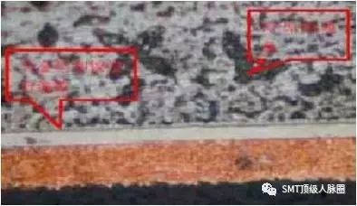
This indicates that there is no problem with the solderability of the PCB and components; the fundamental reason for this phenomenon is that the soldering temperature conditions are inappropriate.
2. Mechanism
The main cause of cold soldering is insufficient heat supply during soldering, where the soldering temperature does not reach the wetting temperature of the solder, resulting in no formation of IMC or an excessively thin IMC, as shown in Figure 2. In some cases, there are also cracks on the interface, as shown in Figure 3.
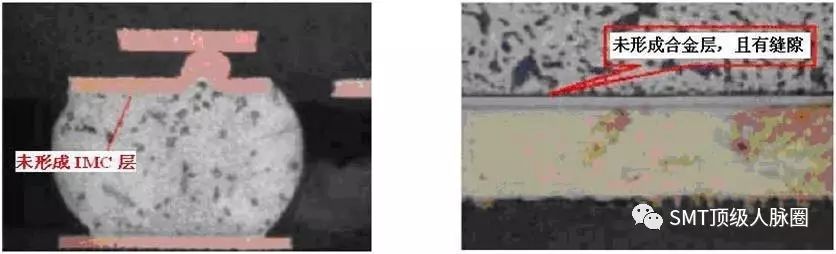
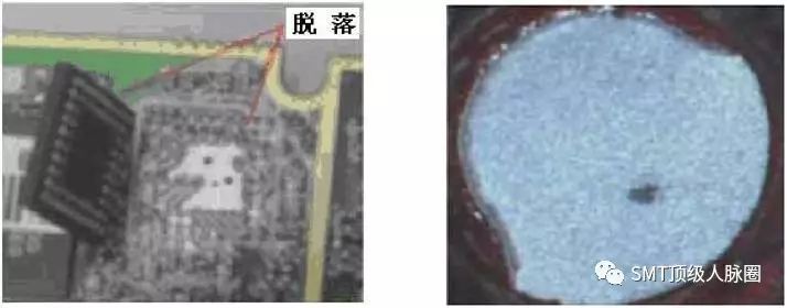
In this case, the solder is adhered to the surface of the pad, sometimes exhibiting no connection strength whatsoever. Figure 4 shows a CSP chip on a PCBA that, due to cold soldering, tears off when subjected to force. After the device separates from the pad, the pad surface is clean and metallic, as shown in Figure 5. This is completely different from the pad surface of a separated cold solder joint.
Cold solder joint criteria include incomplete IMC growth, an orange peel surface, and insufficient collapse height, which are three typical characteristics of cold solder joints in BGA and CSP. These characteristics can usually serve as criteria for identifying cold solder joints in BGA and CSP.
1) In reflow soldering, incomplete IMC growth (previously analyzed and introduced, not repeated here)
2) Orange peel surface and insufficient collapse height
The surface of cold solder joints in BGA and CSP presents an orange peel texture and insufficient collapse height, which is a unique physical phenomenon of cold soldering. The formation mechanism can be described as follows:
During reflow soldering of BGA and CSP, due to the combined effects of gravity and surface tension of the package, they typically undergo the following stages: Stage A begins heating – Stage B first collapse -> Stage C second collapse, as shown in Figure 6.
If the reflow soldering process only reaches Stage B’s first collapse due to insufficient heat supply and cannot continue to Stage C, cold solder joints will form.
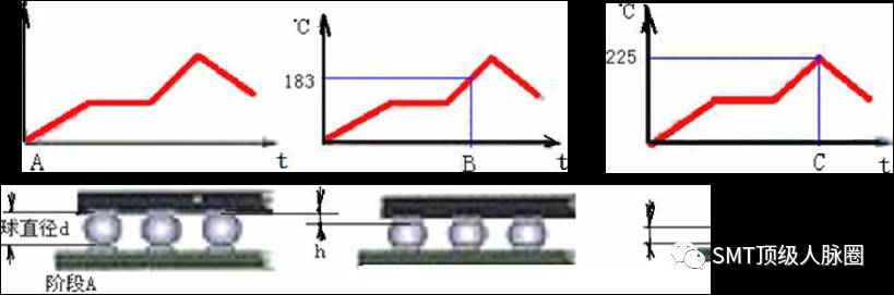
Figure 6 Physical and Chemical Process of BGA and CSP Reflow Soldering
(1) Stage A
At the beginning of heating, the morphology of the BGA and CSP solder joints is shown in Figure 7.
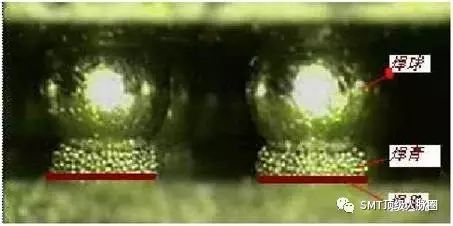
(2) Stage B
After the first stage of heating, the solder ball, when approaching and passing the melting point temperature, will undergo a vertical collapse, and the diameter will begin to increase. At this point, the solder is in a paste-like state with both liquid and solid phases. Due to insufficient heat, the metallurgical reaction between the solder ball and the pad is very weak, and the solder ball surface is rough and dull, as shown in Figure 8.
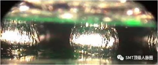
(3) Stage C
Upon further heating, when the solder ball reaches the peak temperature, metallurgical reactions begin to occur between the solder ball and the pad, resulting in a second collapse. At this point, the solder ball flattens, forming a horizontal disc shape, and the surface presents a smooth and shiny structure. The formation of the interfacial alloy layer greatly improves the mechanical strength and electrical performance of the solder joint. At this point, the height of the chip from the board is reduced by 1/3 to 1/2 compared to the initial height, as shown in Figure 9.
From the physical and chemical processes described above during reflow soldering of BGA and CSP, it can be seen that the formation of cold solder joints almost always occurs during the B stage of reflow soldering due to insufficient heating. The reflow soldering process ends before reaching the peak temperature, leading to the formation of cold solder joints. Therefore, when using a micro-optical vision system to inspect the quality of BGA and CSP solder joints, the degree of cold soldering can be assessed based on the surface texture of the solder ball and the collapse height.
4. Analysis of Cold Solder Joint Defects
Slight cold soldering is a hidden defect that will not significantly affect the normal function of the product in a good usage environment for a period of time. This is because the growth of IMC is not only a function of temperature but also related to time. Although the IMC may not develop perfectly during reflow soldering, it can continue to grow and develop during use, albeit at a very slow growth rate. To accurately locate and assess the degree of cold soldering, we classify it into three levels based on the visual characteristics observed by ERSACOPE: Class A (slight cold soldering), Class B (moderate cold soldering), and Class C (severe cold soldering), as shown in Figure 10.
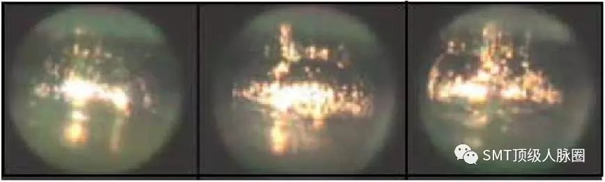
Based on actual observations, Classes A and B are the most common. Further metallographic section analysis of Classes A, B, and C solder joints yields the following results.
1) Class A
The image of the section analysis of Class A solder joints is shown in Figure 11, where the formation of the interfacial IMC (alloy) is not obvious, exhibiting characteristics of cold soldering, but the interface is tightly bonded, with no micro-cracks observed.
5. Causes of Cold Soldering and Countermeasures
1) Reasons for High Cold Soldering Rate in BGA and CSP during Hot Air Reflow Soldering
Hot air convection uses air as a medium for heat conduction, which is ideal for heating components that “protrude” from the PCB, such as high-pin and small components. However, during this process, the influence of the “boundary layer” formed between the convective air and the PCB makes it difficult for hot air to penetrate into the bottom gaps of BGA and CSP, as the gap between the BGA, CSP, and the PCB surface approaches the thickness of the boundary layer. This significantly reduces the thermal conductivity when heat is transmitted to the solder pad areas of BGA and CSP, as shown in Figure 14.

In the above state, during the reflow soldering process of BGA and CSP, heat transfer can only occur by first heating the BGA, CSP packaging and the PCB, and then relying on the packaging and PCB substrate to conduct heat to the solder pads and solder balls of BGA and CSP to form solder joints. For example, if 240°C hot air acts on the surface of the packaging, the solder pad and BGA, CSP solder balls will gradually heat up, with the temperature rise lagging compared to other components. If the required wetting temperature is not reached within the required reflow time, cold soldering will occur.
2) Possible Measures to Reduce Cold Soldering Rate in BGA and CSP
(1) Use a trapezoidal temperature curve (extend peak temperature time)
Appropriately lowering the reflow peak temperature while extending the peak temperature time can improve the temperature difference between components with different heat capacities and avoid overheating of smaller components.
A modern composite reflow soldering system can reduce the temperature difference between a 45mm BGA and small pin packages (SOP) to 8°C.
(2) Improve the heat supply method during reflow soldering
Reflow soldering involves soldering thousands of components onto a PCB substrate. If a PCB has components of varying sizes, heat capacities, and areas, temperature non-uniformity will occur. Currently, this heating method is less efficient than infrared heating in terms of heat exchange, leading to lower production efficiency and higher energy consumption. Additionally, due to poor thermal conductivity, the differences in heating rates between components of different sizes will increase.
The convection speed of circulating gas in forced hot air convection reflow soldering equipment is crucial. To ensure that the circulating gas can act on any area of the PCB, the airflow must have sufficient speed or pressure. This can lead to issues such as vibration of thin PCBs and displacement of components.
② Infrared heating. Infrared (IR) is electromagnetic waves with a wavelength of 3 to 10 μm. Typically, materials such as PCBs, soldering aids, and component packaging are composed of molecular layers bonded by atomic chemistry. These high molecular materials continuously vibrate due to molecular stretching and angle changes. When the vibration frequency of these molecules comes into contact with nearby infrared electromagnetic waves, resonance occurs, leading to more intense vibrations. Frequent vibrations generate heat, allowing thermal energy to be rapidly and evenly distributed throughout the object in a short time. Therefore, the object does not need to be subjected to high temperatures from the outside.
The advantages of infrared heating for reflow soldering include: uniform heating across the surface of the same object, minimal thermal stress generated by the soldered parts, high thermal efficiency, and energy savings.
However, its disadvantages include: due to varying surface reflectivity and material properties of the objects being heated, there can be temperature differences between them, and some objects may overheat due to excessive absorption of heat.
③ “IR + Forced Convection” is the main technical means to solve the issue of cold soldering in BGA and CSP. In foreign industries, it has been found that when heating QFP140P and PCB, as well as 45mm BGA and PCB, with only convection heating or the “IR + Forced Convection” composite heating system, the temperature uniformity under both conditions differs as follows:
a) Convection heating shows a temperature difference of 22°C between QFP140P and PCB;
b) “IR + Forced Convection” heating shows a temperature difference of only 7°C between QFP140P and PCB, and the temperature difference for the 45mm BGA further reduces to 3°C.
The basic concept of “IR + Forced Convection” heating is to use infrared as the primary heat source to achieve optimal thermal conduction while leveraging the balanced heating characteristics of convection to reduce the temperature difference between components and the PCB. The convection heating method is beneficial when heating large-capacity components and helps cool smaller heat capacity components when they overheat.
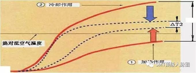
① Represents the heating curve of components with large heat capacities;
② Is the heating curve of small heat capacity components.
If only one heat source is used, whether it is IR or convection, the heating effect will occur as shown by the solid line in Figure 17. The two dashed lines describe the heating curves of the “IR + Forced Convection” composite heating’s advantages (AT2 < AT1). The role of adding forced convection is to heat components below the hot air temperature while helping to cool components that have already risen above the hot air temperature.
The most advanced reflow oven technology currently combines the advantages of both convection and infrared radiation heating. The maximum temperature difference between components can be maintained within 8°C, while the temperature difference between PCBs can be stabilized at about 1°C during continuous mass production.
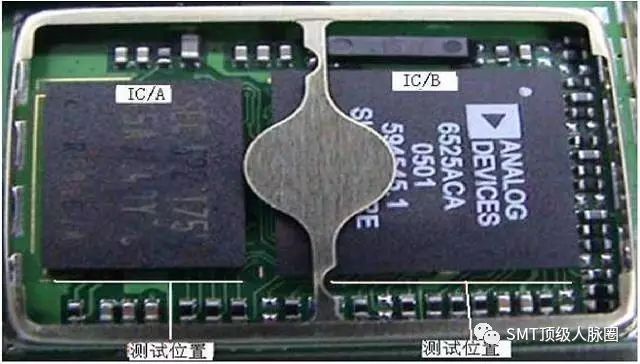
The occurrence of cold soldering phenomena in BGA and CSP is also significantly related to their installation positions on the PCB. Figure 168 shows two CSP chips (IC/A and IC/B) installed together within a shield, where chip IC/A is smaller and thinner than chip IC/B, and there is a larger gap between it and the shield. From the effect of hot air reflow soldering, IC/A should perform better than chip IC/B.