


Most Popular, Active, and Influential in the SMT Industry
WeChat Official Account — SMT Top Networking Circle
First Media for Mobile Internet Marketing in SMT Manufacturing
SMT Top
Networking Circle
1. What are the inspection standards for PCBA boards?
First, let us understand the introduction of quality inspection standards.
1. Serious defects (CR): Any defect that can cause harm to human beings or machines or endanger life safety, such as: non-compliance with safety regulations / burning machines / electric shock, etc.
2. Major defects (MA): Defects that may cause product damage, functional abnormalities, or affect the product’s lifespan due to materials.
3. Minor defects (MI): Defects that do not affect product functionality and lifespan, such as some appearance flaws and slight assembly issues or differences.
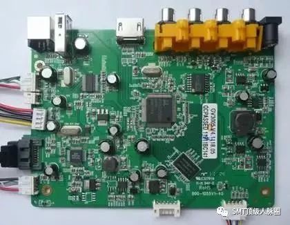
What items need to be inspected for PCBA boards and what are the inspection standards?
2. Inspection conditions for PCBA boards:
1. To prevent contamination of components or parts, gloves or finger cots with full EOS/ESD protection must be selected, and static rings must be worn during operation. The light source should be white daylight lamps, with light intensity above 100 Lux, clearly visible within 10 seconds.
2. Inspection method: Place the item to be inspected about 40cm from the eyes, at an angle of 45 degrees up and down, left and right, and inspect with the naked eye or a threefold magnifying glass.
3. Inspection determination standards: (Sampling based on QS9000 C=0 AQL=0.4%; if the customer has special requirements, determine according to customer acceptance standards)
4. Sampling plan: MIL-STD-105E LEVEL II normal single sampling.
5. Determination standards: Serious defects (CR) AQL 0%.
6. Major defects (MA) AQL 0.4%.
7. Minor defects (MI) AQL 0.65%.
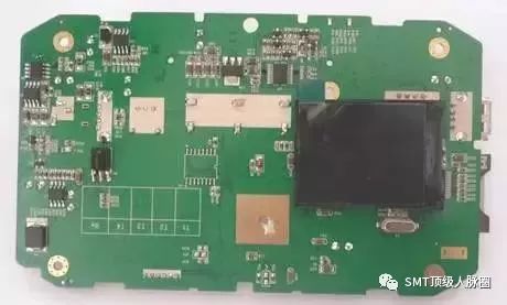
Inspection item standards for PCBA boards in the SMT patch workshop.
3. Inspection item standards for PCBA boards in the SMT patch workshop
01. SMT component solder joint open solder.
02. SMT component solder joint cold solder: Use a toothpick to gently push the component leads; if it can be moved, it is cold solder.
03. SMT component (solder joint) short circuit (solder bridge).
04. SMT component missing.
05. SMT component wrong part.
06. SMT component polarity reversed or wrong, causing burning or explosion.
07. SMT component multiple parts.
08. SMT component upside down: text side facing down.
09. SMT component standing sideways: chip components with length ≤3mm, width ≤1.5mm, no more than five (MI).
10. SMT component tombstone: ends of chip components lifted up.
11. SMT component lead offset: side offset less than or equal to half the width of the solderable end.
12. SMT component floating high: distance between component bottom and substrate.
13. SMT component lead high lift: lift height greater than the thickness of the lead.
14. SMT component lead not flat: lead not soldered.
15. SMT component not identifiable (printing blurred).
16. SMT component lead or body oxidation.
17. SMT component body damaged: capacitor damaged (MA); resistor damaged less than 1/4 of component width or thickness (MI); IC damaged in any direction longer than.
18. SMT component using non-designated suppliers: according to BOM, ECN.
19. SMT component solder joint solder spike: solder spike height greater than the body height of the component.
20. SMT component insufficient solder: minimum solder point height less than solder thickness plus solderable end height of 25% or solder thickness plus 0.5mm, whichever is smaller (MA).
21. SMT component excessive solder: maximum solder point height exceeds the pad or extends to the top of the metal plating end cap solderable end is acceptable, solder touching the component body (MA).
22. Solder balls/solder dross: more than 5 solder balls or solder splashes (0.13mm or smaller) per 600mm2 (MA).
23. Solder joint has pinholes/blowholes: one solder joint has one (or more) (MI).
24. Crystallization phenomenon: white residues on the surface of the PCB board, white crystallization on the metal surface around the soldering terminal.
25. Unclean board surface: uncleanliness that cannot be detected within a distance of 30 seconds is acceptable.
26. Poor glue dispensing: glue located in the solder area, reducing the width of the solderable end by more than 50%.
27. PCB copper foil peeling.
28. PCB exposed copper: exposed copper width greater than 0.5mm (MA).
29. PCB scratches: scratches that do not reveal the substrate.
30. PCB yellowing: PCB that has been through a reflow oven or repaired showing burnt yellowing different from the PCB color.
31. PCB bending: any direction of bending exceeding 1mm (300:1) every 300mm (MA).
32. PCB inner layer separation (bubbles): areas with bubbling and delamination do not exceed 25% of the distance between plated holes or internal wires (MI); bubbling between plated holes or internal wires (MA).
33. PCB contamination: conductive (MA); non-conductive (MI).
34. PCB version error: according to BOM, ECN.
35. Gold finger soldering: soldering positions within 80% from the edge of the board (MA).
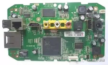
Inspection item standards for PCBA boards in the DIP post-soldering workshop.
4. Inspection item standards for PCBA boards in the DIP post-soldering workshop
01. DIP component solder joint open solder.
02. DIP component solder joint cold solder: Use a toothpick to gently push the component leads; if it can be moved, it is cold solder.
03. DIP component (solder joint) short circuit (solder bridge).
04. DIP component missing.
05. DIP component lead length: Φ≤0.8mm→lead length less than or equal to 1.5mm; Φ>0.8mm→lead length less than or equal to 2.0mm special cut lead requirements excluded.
06. DIP component wrong part.
07. DIP component polarity reversed or wrong, causing burning or explosion.
08. DIP component lead deformation: lead bent more than 50% of lead thickness.
09. DIP component floating high or high lift: refer to IPC-A-610E, depending on assembly and special circumstances.
10. DIP component solder joint solder spike: solder spike height greater than 1.5mm.
11. DIP component not identifiable (printing blurred).
12. DIP component lead or body oxidation.
13. DIP component body damaged: surface damage without exposing the internal metal material.
14. DIP component using non-designated suppliers: according to BOM, ECN.
15. PTH hole vertical filling and surrounding wetting: at least 75% vertical filling, lead and hole wall at least 270° wetting.
16. Solder balls/solder dross: more than 5 solder balls or solder splashes (0.13mm or smaller) per 600mm2 (MA).
17. Solder joint has pinholes/blowholes: one solder joint has three (or more) (MI).
18. Crystallization phenomenon: white residues on the surface of the PCB board, white crystallization on the metal surface around the soldering terminal.
19. Unclean board surface: uncleanliness that cannot be detected within a distance of 30 seconds is acceptable.
20. Poor glue dispensing: glue located in the solder area, reducing the width of the solderable end by more than 50%.
21. PCB copper foil peeling.
22. PCB exposed copper: exposed copper width greater than 0.5mm (MA).
23. PCB scratches: scratches that do not reveal the substrate.
24. PCB yellowing: PCB that has been through a reflow oven or repaired showing burnt yellowing different from the PCB color.
25. PCB bending: any direction of bending exceeding 1mm (300:1) every 300mm (MA).
26. PCB inner layer separation (bubbles): areas with bubbling and delamination do not exceed 25% of the distance between plated holes or internal wires (MI); bubbling between plated holes or internal wires (MA).
27. PCB contamination: conductive (MA); non-conductive (MI).
28. PCB version error: according to BOM, ECN.
29. Gold finger soldering: soldering positions within 80% from the edge of the board (MA)

Continuous learning and improvement
is the way to meet a better self.
10 million SMT professionals in China
Recommended WeChat Official Account that you will love:
A SMT circle that gathers millions of connections
▲ Long press the QR code to “recognize” and follow ▲
Disclaimer: The copyright of articles, images, audio, video files, etc. reprinted by this public account belongs to the copyright owner. The purpose of reprinting is to convey more information and does not represent this public account’s endorsement of their viewpoints or responsibility for their authenticity. If the original author believes that their work is not suitable for browsing or should not be used free of charge, please contact us promptly to take immediate action to avoid unnecessary losses to both parties.
Welcome to share in your circle of friends, every repost is the greatest support and encouragement for us!
