 WeChat Official Account:Electromagnetic Compatibility HomeIntroduction
It should be noted that this summary only provides some basic conclusions. Specific calculations for trace lengths of frequency signals, harmonic frequencies to consider, wavelength, PCB-level shielding, design of shielding cavities, size and number of shielding apertures, handling of incoming and outgoing wires, calculations for cutoff waveguide diameters and lengths, as well as knowledge on electrostatic protection, lightning protection, etc., are not described. Some conclusions may not be entirely correct, and corrections are welcome; I would be very grateful.
1. Component Layout
When designing EMC for printed circuit boards, layout must be considered first. PCB engineers must coordinate with structural engineers and EMC engineers to balance both aspects to achieve optimal results.
First, consider the structural dimensions of the printed circuit board and how to arrange the components. If the components are widely distributed, the transmission lines between them may be long, leading to longer printed traces, increased impedance, reduced noise immunity, and higher costs. Conversely, if the components are too closely packed, heat dissipation will be poor, and adjacent traces may be susceptible to coupling and crosstalk. Therefore, a comprehensive layout of all components based on the functional units of the circuit should be performed, taking into account electromagnetic compatibility, thermal distribution, sensitive and non-sensitive components, I/O interfaces, reset circuits, clock systems, and other factors.
Generally, the following basic principles should be followed during overall layout:
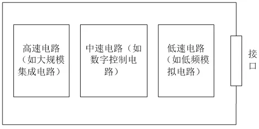
1. When high, medium, and low-speed circuits coexist on the same board, they should be logically segmented: when arranging fast, medium, and slow logic circuits, high-speed components (fast logic, clock oscillators, etc.) should be placed close to the connectors to reduce antenna effects, while low-speed logic and memory should be placed further away from the connectors. This is beneficial for reducing common impedance coupling, radiation, and interference.
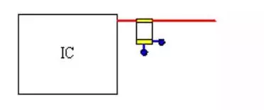
2. In single-sided or double-sided boards, if the power line routing is long, decoupling capacitors should be added to ground every 3000 mil, with capacitance values of 10uF + 1000pF to filter out high-frequency noise on the power line.
3. In single-sided and double-sided boards, the routing of filter capacitors should first go through the filter capacitor for filtering before reaching the component pins, ensuring that the power voltage is filtered before supplying power to the IC, and the noise fed back to the power supply by the IC will also be filtered out by the capacitor first. The placement of decoupling capacitors should be determined based on actual conditions; they do not necessarily have to be placed at the positive terminal of the power supply but can also be placed at the negative terminal, with the principle of ensuring minimal ground impedance.
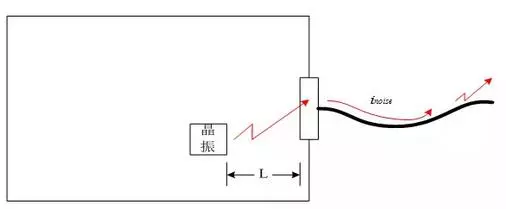
4. Clock lines, buses, RF lines, and other strong radiation signal lines should be kept at least 1000 mil away from outgoing signal lines to avoid interference coupling from strong radiation signal lines to outgoing signal lines, which could lead to external radiation. Components such as crystals, oscillators, relays, and switching power supplies are strong radiators and should be carefully considered during layout.
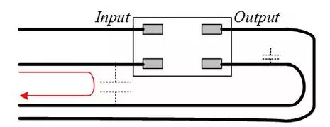
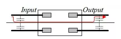
5. The input and output signal lines of filters (filter circuits) should not run parallel or cross each other to avoid direct noise coupling between the lines before and after filtering.
6. For series matching resistors at the starting end, they should be placed close to their signal output end, i.e., near the driving source.

7. Each filter capacitor for IC filtering should be placed as close as possible to the chip’s power pins to reduce the high-frequency loop area, thereby minimizing radiation.
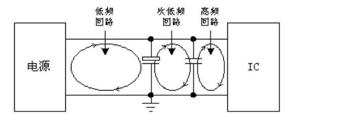
8. On the PCB, the filtering, protection, and isolation devices of the interface circuit should be placed close to the interface and follow the principle of protection before filtering.
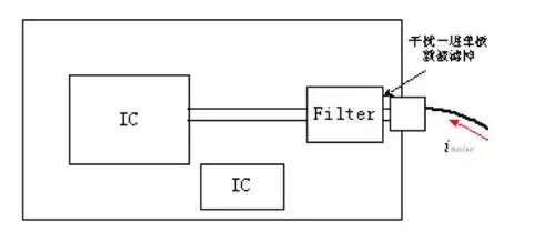
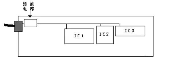
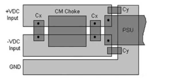
9. The filtering circuit for the power input of the PCB should be placed close to the interface.
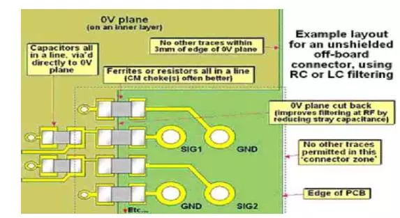
10. When the interface circuit uses isolation for filtering design, its RC and LC circuits should adopt the following layout, and no other traces are allowed in the isolation area.
11. No components are allowed to be placed within 4mm of the edge of the PCB.
12. Arrange the positions of various functional circuit units according to the direction of signal flow, making the layout conducive to signal circulation and keeping the signal direction as consistent as possible, with the shortest signal traces and no return paths.
13. Layout should be centered around the core components of each functional circuit. Components should be arranged uniformly, neatly, and compactly on the PCB, minimizing and shortening the leads and connections between components.
14. For high-frequency circuits, the distribution parameters between components should be considered. Generally, components should be arranged in the same direction as much as possible.
15. Minimize the parameters between high-frequency components to reduce their distribution parameters and mutual electromagnetic interference. Components that are easily interfered with should not be placed too close to each other, and input and output components should be as far apart as possible.
16. The positions of components should be grouped according to power voltage, digital and analog circuits, speed, and current size to avoid mutual interference. The arrangement of connector pins on the printed board can be determined based on the positions of the components. All connectors should be arranged on one side of the printed board to minimize cable leads from both sides, reducing common-mode radiation.
17. High-frequency filter capacitors must be placed near the power pins of each IC to reduce ground loops, and each power pin should have a high-frequency small capacitor.
18. Energy storage capacitors and high-frequency filter capacitors should be placed near circuit units or components that experience significant current changes (e.g., I/O of power modules, fans, and relays).
2. PCB Routing
When routing on the PCB, first determine the positions of the components on the board, then arrange the ground lines and power lines, followed by high-speed signal lines, and finally consider low-speed signal lines. Ground lines should be routed first; this rule is very important, and ground lines are best arranged in a mesh layout.
1. Power lines: Under safety considerations, power lines should be as close as possible to ground lines to minimize the loop area of differential mode radiation, which also helps reduce circuit interference.
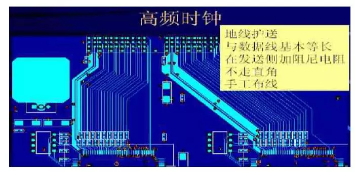
2. The positions of clock lines, signal lines, and ground lines: The distance between signal lines and ground lines should be close to minimize the loop area formed. The clock lines should be surrounded by ground lines as much as possible to prevent clock signals from interfering with other signals, and the surrounding ground lines should connect to the ground plane with as many vias as possible to reduce ground impedance and prevent the ground line from becoming an emitting antenna.
◇ Grounding treatment for clock lines
3. Clock lines and signal lines should avoid layer changes; if a layer change is necessary due to practical circumstances, a ground via should be placed at the via location.
◇ Ground vias at clock line and signal line via locations

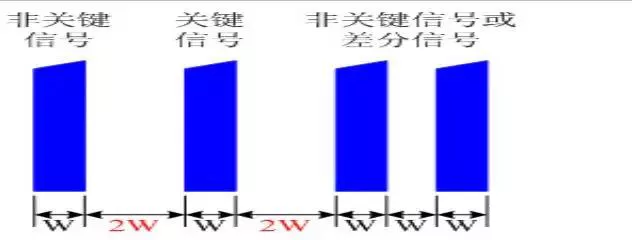
4. Key signal routing such as clock lines, buses, RF lines, and other critical signal lines should meet the 3W principle when running parallel to other lines on the same layer.
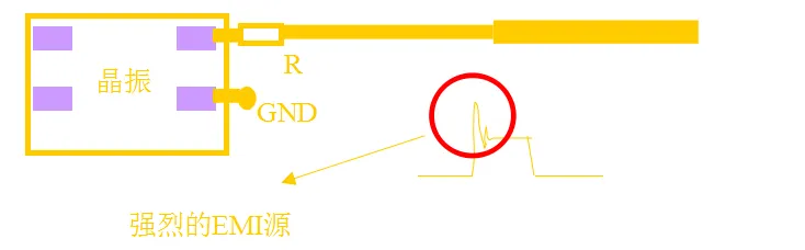
5. Avoid discontinuities in PCB traces: ◇ Trace widths should not change abruptly ◇ Traces should not have sudden corners; signal routing should avoid “hairy edges,” “sharp angles,” “right angles,” and “inconsistent widths.”
◇ Traces should not have sudden corners

◇ Trace widths should not change abruptly
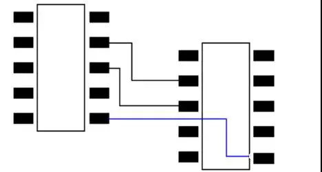
6. Input and output lines should avoid being adjacent over long distances to reduce crosstalk between inputs and outputs (except for differential pairs).
7. There should be no unrelated signal traces beneath the filter (filter circuit) on the PCB.
8. Crystal oscillator traces should be as close as possible to the IC, and ground treatment should be applied on both sides of the clock line. The clock ground pin should be directly connected to the CPU ground pin on the same layer to reduce the ground loop of the crystal oscillator. The width of the clock line should be at least 10 mil, and the width of the escort ground line should be at least 20 mil. It is best to expose the ground copper under the clock crystal to increase capacitive coupling.
9. Key signal lines (such as clock lines, buses, interface signal lines, RF lines, reset lines, chip select lines) are generally strong radiation sources or sensitive signal lines and should be routed as close to the ground plane as possible to reduce their signal loop area, thereby decreasing their radiation intensity or improving their anti-interference capability.
10. High-frequency signal lines should be kept away from clock or crystal oscillator traces; clock lines and high-speed signal lines should avoid running parallel to each other. If parallel routing is necessary due to practical circumstances, ground lines should be used to separate them.
11. Key signal lines should not cross partition lines; if crossing is necessary, bridging methods should be used nearby to ensure the signal forms a complete loop.
12. The highest principle in routing should be to minimize the return loop area.
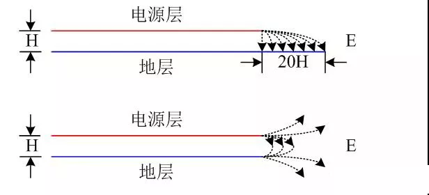
13. The power plane should be recessed 20H relative to its adjacent ground plane; if structural limitations exist, it should still ensure 5H.
14. Signal lines and address lines should avoid forming ground rows or ground trenches.
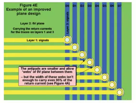 3. EMC Design of Power Supply
The EMC design of the power supply includes not only the EMC design of switching power supplies but also the EMC design of power supplies for digital and analog circuits.
The EMC design of switching power supplies mainly includes the design of common mode filters, differential mode filters, parameter design of switching transformer buffer circuits, design of absorption circuits for switching transistors and fast diodes, and shielding design of switching transformers, among other projects. Specific designs should be based on the specific product.
The EMC design of the power supply section for analog and digital circuits is a very important part, mainly including the selection of BULK decoupling capacitors, IC decoupling capacitors, overall decoupling capacitors, ferrite beads, and filtering methods.
The AC loop of the power switch and the AC loop of the rectifier contain high amplitude trapezoidal currents, which have a high harmonic content, with frequencies much greater than the switching fundamental frequency. The peak amplitude can be as high as five times the sustained input/output DC current amplitude, with a transition time typically of 50ns. These two loops are the most likely to generate electromagnetic interference. Therefore, priority should be given to routing these loops, ensuring that the three main components in each loop: filter capacitors, power switches or rectifiers, and inductors or transformers are set adjacent to each other, adjusting the positions of components to keep the current loop paths as short as possible.
The wiring rules for switching power supplies are as follows:
1. All leads carrying AC signals should be as short and wide as possible.
2. Minimize loop area to suppress radiation interference from switching power supplies.
3. Based on the size of the printed circuit board current, increase the width of the power lines as much as possible to reduce loop resistance.
4. The routing of power lines and ground lines should be consistent with the direction of current flow to increase noise immunity.
The grounding design rules for switching power supplies are as follows:
1. Usually, single-point grounding is chosen: the common terminal of the input filter capacitor should be the only connection point for coupling to the large current AC ground, and the grounding points of the same level circuit should be as close as possible. The filter capacitor of this level circuit should be connected to this level grounding point, mainly considering that the return currents from various parts of the circuit to ground are variable.
2. Ground lines should be thickened as much as possible: the width of the ground line should ideally be wider than that of the power line; if possible, the width of the ground line should exceed 3mm. Large area copper layers can also be used as ground lines, connecting all unused areas on the printed board to ground.
3. Grounding design for control chips: power ground and signal ground should ultimately converge to a single ground, but power ground and power supply ground should form a return path, while signal ground should form a return path with signal lines. Power ground and signal ground should not be confused, and they should ultimately achieve single-point grounding. The IC control ground should be placed after the layout of other AC circuit loops is completed, and the control ground should connect to the main power ground through a specific point to reduce noise introduced by connections between the detection part, error amplifier, and sensitive input terminals.
4. EMC Design of Digital Circuits
The EMC design of digital circuits mainly includes the selection of active devices, EMC design of clock circuits, EMC design of data buses and address buses, impedance matching and ground bounce design, and filtering design for bus drivers.
First, attention should be paid to the selection of devices: devices with smooth rising edges should be prioritized. High-speed digital device routing is prone to ringing, which typically manifests as harmonic emissions. A common solution is to place a damping resistor or a ferrite bead in series on high-speed data lines.
90% of EMI is caused by 10% of critical circuits, so special attention should be paid to the routing of critical circuits during layout. Critical circuits mainly include clock circuits, high-speed data buses, address buses, reset lines, relay lines, control lines, etc., and these key lines should be prioritized during routing.
The grounding design for high-speed data circuits is generally multi-point grounding to reduce ground impedance.
The power design for high-speed data circuits is as follows:
Decoupling at the power entry point of the circuit board: Most circuit boards’ power entry points include a large decoupling electrolytic capacitor and one or two small high-frequency decoupling capacitors, mainly to provide recharging for digital circuits while reducing high-frequency noise.
Device decoupling: Any clock-controlled device (except microprocessors) must have high-speed capacitors decoupled at the power pins. If multiple power and ground pins are provided, decoupling capacitors must be added to all of them.
The routing rules for high-speed data circuits are as follows:
1. The positions of clock lines, signal lines, and ground lines: The distance between signal lines and ground lines should be close to minimize the loop area formed. Clock lines should be surrounded by ground lines as much as possible to prevent clock signals from interfering with other signals, and the surrounding ground lines should connect to the ground plane with as many vias as possible to reduce ground impedance and prevent the ground line from becoming an emitting antenna.
2. Logical speed segmentation: When arranging fast, medium, and slow logic circuits on the circuit board, high-speed components (fast logic, clock oscillators, etc.) should be placed close to the connector range to reduce antenna effects, while low-speed logic and memory should be placed further away from the connector range. This is beneficial for reducing common impedance coupling, radiation, and interference.
3. Avoid discontinuities in PCB traces: ◇ Trace widths should not change abruptly ◇ Traces should not have sudden corners.
4. Input and output lines should not be placed too close to clock lines, oscillator lines, power lines, and other electromagnetic lines, nor should they be placed too close to reset lines, interrupt lines, control lines, and other sensitive signal lines. Long-distance adjacency should be avoided to reduce crosstalk between inputs and outputs (except for differential pairs).
5. Signal routing should avoid “hairy edges,” “sharp angles,” “right angles,” and “inconsistent widths.”
6. Crystal oscillator traces should be as close as possible to the IC, and ground treatment should be applied on both sides of the clock line. The clock ground pin should be directly connected to the CPU ground pin on the same layer to reduce the ground loop of the crystal oscillator. The width of the clock line should be at least 10 mil, and the width of the escort ground line should be at least 20 mil.
7. Key signal lines (such as clock lines, buses, interface signal lines, RF lines, reset lines, chip select lines) are generally strong radiation sources or sensitive signal lines and should be routed as close to the ground plane as possible to reduce their signal loop area, thereby decreasing their radiation intensity or improving their anti-interference capability.
8. High-frequency signal lines should be kept away from clock or crystal oscillator traces; clock lines and high-speed signal lines should avoid running parallel to each other. If parallel routing is necessary due to practical circumstances, ground lines should be used to separate them.
9. Clock lines and signal lines should avoid layer changes; if a layer change is necessary due to practical circumstances, a ground via should be placed at the via location.
10. Differential signal lines should be on the same layer, of equal length, and run in parallel, maintaining consistent impedance; there should be no other traces between differential pairs. If vias are necessary due to practical circumstances, they should be placed simultaneously and not too far apart.
11. Key signal lines should not cross partition lines; if crossing is necessary, bridging methods should be used nearby to ensure the signal forms a complete loop.
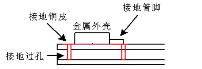
12. Devices with grounded metal shells, such as crystals, should have grounding copper laid on the top layer of their projection area to suppress external radiation and improve anti-interference capability through the distributed capacitance between the metal shell and the grounding copper.
5. EMC Design of Analog Circuits
The EMC design of analog circuits mainly considers EMS, as analog devices are very sensitive to interference. Therefore, the EMC design of analog circuits mainly involves adding protective devices at necessary ports to suppress external electronic interference. Common protective devices include filtering devices, ferrite beads, transient suppression diodes, common mode chokes, isolation transformers, etc.
Analog circuits operate at low frequencies, and any mv-level voltage change can alter their operating state. Therefore, the EMC design of analog circuits mainly considers EMS, and single-point grounding is the best grounding method for these sensitive circuits. The main purpose of grounding is to prevent large grounding currents from other noise sources, such as digital circuits, switching power supplies, and relays, from competing with sensitive analog ground lines. Ground loops must avoid all sensitive low-frequency analog circuits.
For mixed-signal circuits, it is best not to perform ground splitting. With the rapid development of chips, most chips now contain both digital and analog circuits. In this case, it is best to mix digital ground and analog ground while concentrating the peripheral devices of the analog part in the layout, away from interference sources.
6. EMC Design of Interface Circuits
The EMC design of interface circuits includes the design of filtering circuits and protective circuits for interface circuits.
The purpose of interface circuit filtering design is to reduce the radiation generated by the system through interfaces and cables, suppress external radiation and conducted noise interference to the entire system.
The purpose of interface protection circuit design is to ensure that the circuit can withstand certain overvoltage and overcurrent impacts.
The design of interface filtering circuits and protective circuits should follow the basic design principles below:
1. The impact of filtering and protective circuits on interface signal quality must meet requirements.
2. Filtering and protective circuits should be designed based on actual needs and should not be simply copied.
3. When filtering and protective circuits need to be implemented simultaneously, the principle of protection before filtering should be ensured.
4. Interface chips, including corresponding filtering, protection, and isolation devices, should be placed as linearly as possible along the signal flow direction at the interface connector.
5. Filtering, protection, and isolation devices for interface signals should be placed as close as possible to the interface connector, and the corresponding signal connection lines must be as short as possible (the shortest distance under process requirements).
6. Interface transformers should be placed close to the connector, typically within 3cm of the corresponding interface connector.
7. Analog signal interfaces and digital signal interfaces, low-speed logic signal interfaces and high-speed logic signal interfaces, etc. (distinguished by sensitivity and interference emission levels) should be spaced apart. When there is a possibility of mutual interference between connectors, isolation and shielding measures must be taken.
8. When different types of signals exist within the same interface connector, ground pins must be used to isolate these signals, especially for some sensitive signals.
9. The width of interface signal lines should always be consistent. For high-speed signal lines, if routing requires bending, smooth arc bends should be used.
10. No other signal lines should be routed between differential lines and signal return lines; the corresponding parts of differential pairs should run parallel, close together, and on the same layer, with lengths kept as consistent as possible.
11. When interface signal lines are long (exceeding 2.5cm from the driver or receiver to the interface connector), routing methods should be used to ensure that the traces meet the specified characteristic impedance.
12. All signal traces should not cross plane traces unless they have passed through isolation filters.
13. It is recommended to use connectors with shielded housings for interface signal lines, especially for high-frequency signal connectors.
14. The metal shell of the connector should maintain good electrical continuity with the chassis; for connectors that can be surrounded 360 degrees, they must be connected 360 degrees, and the connection impedance should typically be less than 1mΩ.
15. For connectors that cannot be connected 360 degrees, it is recommended to use connectors with spring clips around the shell, and the clips must have sufficient size and performance (elasticity) to maintain good electrical connection with the chassis.
16. Filtering connectors can significantly help the EMC performance of products, but they are relatively expensive. Generally, filtering connectors are not used when problems can be solved with internal filtering or cable shielding.
17. The shielding layer of shielded wires should maintain 360-degree connection with the connector housing as much as possible. For interfaces that cannot achieve this, other corresponding measures should be taken to ensure the EMC performance of the interface.
18. Interface signal lines and interface chips must comply with the requirements of suppliers or standards for impedance matching, filtering, isolation, and protection.
7. Structural EMC Design
Structural EMC design includes several scenarios such as the bottom plate, chassis, and internal routing of the device.
The bottom plate and chassis are the most effective methods for providing shielding against unwanted signal pathways in control devices or functional units. Therefore, the bottom plate and chassis of electronic products should preferably be made of metal structures or internally plated metal plastic structures.
Structural gaps must be minimized to reduce structural discontinuities, thereby controlling leakage radiation from the bottom plate and chassis. Structural measures to improve gap shielding effectiveness include increasing gap depth, reducing gap length, adding conductive gaskets at joints, applying conductive coatings at seams, and shortening screw spacing.
The direction of structural openings should align with the direction of magnetic lines; if perpendicular to the magnetic lines, it will cut through the magnetic lines, increasing magnetic resistance and degrading shielding effectiveness.
Disorganized internal routing of devices can render the designed shielding, filtering circuits, and grounding measures ineffective for non-shielded electronic devices. Disorganized internal routing not only causes interference between high and low-level signals but also complicates subsequent remedial measures such as shielding, filtering, and grounding.
The basic principles for internal routing of devices are:
1. Various exposed traces within the chassis should be kept as short as possible.
2. Wires transmitting signals of different levels should be bundled together; digital circuit and analog circuit signal lines should be bundled together and kept at an appropriate distance to reduce mutual influence.
3. Flat cables used for signal transmission in products should be arranged in a ground-signal-ground-signal-ground manner to effectively suppress interference and enhance anti-interference capability.
4. Low-frequency incoming and return lines should be twisted together to form twisted pairs, reducing electromagnetic interference.
5. Wires that are determined to cause significant radiation interference should be shielded.
6. The shielding of shielded cables entering and exiting the shielded enclosure must ensure reliable contact between the shielding layer and the shielded enclosure, generally requiring 360-degree contact and providing sufficiently low contact impedance.
7. Non-shielded cables are generally prohibited from exiting directly from the shielded enclosure. In special cases, direct exit is allowed, but the length of the cable inside the shielded enclosure (or outside) must not exceed 80mm. This dimension includes traces on the PCB; if there is a filtering circuit, it refers to the length of the cable between the filtering circuit and the shielded enclosure.
8. Non-shielded cables can also be treated with a special measure: wrapping the non-shielded cable with a metal mesh inside the shielded enclosure to form a locally shielded cable, which is then treated as a shielded cable. It should be noted that this method may have process limitations and limited effectiveness.
9. Shielded cables have a special application scenario where the shielding layer is not allowed to connect to the shielded enclosure (which is actually PGND). A typical example is coaxial cables. In this case, the shielded cable can be treated as a non-shielded cable (the length on the shielded enclosure side must not exceed 80mm) or use double-shielded cables.
8. Grounding Design
Grounding must first adopt a low-impedance design. Compared to other electrical connection lines, grounding design requires grounding lines to be as thick and short as possible, especially in printed board design, where large area connections are usually adopted. Ground loop issues are also a key consideration in grounding design, but ground loops generally occur in low-frequency scenarios. In most cases, a low-impedance grounding pathway design is used to address such issues.
Ground loops are not a major concern in high-speed circuit design, as they are difficult to eliminate. The focus should be on reducing the impedance of the ground line, so digital circuits often use multi-point grounding. However, for low-frequency analog circuits and small signal circuits, ground loop issues are quite important, and it is essential to minimize ground loop areas to suppress interference on low-frequency analog circuits and small signal circuits.
In digital circuits, their operating characteristics do not depend on the working frequency in the circuit but rather on the rising and falling edges of the working pulses. Therefore, the harmonic frequency band generated by digital circuits is very wide and has a large amplitude, so multi-point grounding is often used to reduce ground impedance.
As IC devices now often contain both analog and digital circuits, a mixed grounding approach of single-point and multi-point grounding is often adopted in design. In digital circuits, multi-point grounding or large area grounding methods are used; in analog circuits, single grounding is used.
In practice, the above grounding methods can be well implemented in printed board design; however, in system design, grounding design becomes more complex due to the need to consider the quality of signal transmission, as well as the system’s requirements for EMS, safety design, and corresponding EMC performance.
Single-point and multi-point grounding are issues of concern for designers. Single-point grounding is suitable for small signal and analog circuits, while multi-point grounding is suitable for high-frequency circuit design. In small signal and analog circuit design, mV-level interference can affect circuit performance, and single-point grounding can control the current path to avoid the formation of ground loops. In high-frequency circuits, lead inductance and parasitic capacitance can disrupt single-point grounding, resulting in high ground impedance and hidden ground loops. Therefore, many engineers often separate digital ground from analog ground, but due to the limitations of printed boards, they cannot fully adhere to EMC design principles, leading to failures in printed board design. The rapid development of modern science and technology and the fast pace of integrated chip development mean that a chip often includes both digital and analog circuits. Even the most experienced PCB engineers may find it difficult to completely separate digital ground from analog ground. To demonstrate whether digital ground and analog ground can be mixed, Tony Waldron, a member of the IEEE, mixed the two grounds into a complete ground during EMC rectification of a large theater, completely solving the microphone hum problem caused by wires over 20 meters long. When the power was turned on, the entire theater was silent, and the engineers present could hardly believe their ears.



Screenshots from some electronic books

Complete set of hardware materials collection