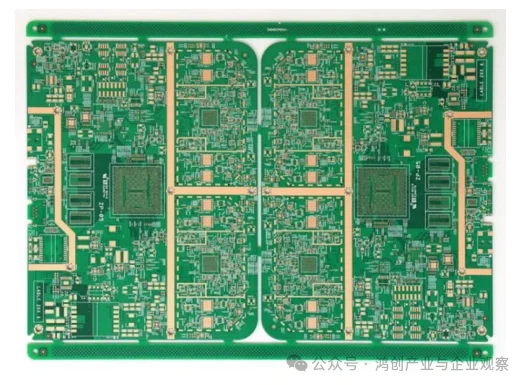
 🔴 A Printed Circuit Board (PCB) is a functional board formed by creating conductive circuit patterns or containing printed components on a copper-clad or general substrate according to a predetermined design. It is used to achieve interconnection and relay transmission between electronic components and serves as the fundamental component for assembling electronic parts. PCBs not only provide electrical connections for electronic components but also support functions such as digital and analog signal transmission, power supply, and RF microwave signal transmission and reception. They are widely used in communication electronics, consumer electronics, computers, data centers, automotive electronics, industrial control, medical devices, and other fields, making them an indispensable component in modern electronic information products, often referred to as the “mother of the electronics industry.”
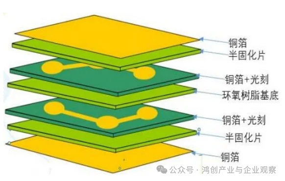 🔵 PCBs can be classified into single-sided, double-sided, multilayer, HDI, flexible boards, IC carrier boards, etc., based on substrate material, product performance, and application fields. A single-sided board refers to a PCB with conductive patterns on only one side of the insulating substrate, mainly used in common household appliances, remote controls, fax machines, etc. A double-sided board has conductive patterns on both sides of the insulating substrate, mainly used in computer peripherals and household appliances. Ordinary multilayer boards consist of four or more layers of conductive patterns and insulating materials pressed together, with the outer layer being copper foil, and inter-layer conductive patterns interconnected through vias. A backplane is a PCB used to connect or plug multiple single boards to form an independent system.
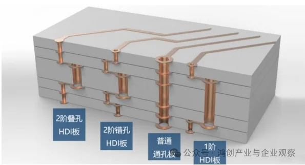 🟠 Metal substrates are composite printed circuit boards consisting of a metal substrate, an insulating medium layer, and a circuit layer, mainly used in communication wireless base stations and microwave communications. Thick copper boards use thick copper foil (copper thickness of 3OZ or more) for PCBs. High-frequency microwave boards are made from special high-frequency materials, mainly used in communication base stations, microwave transmission, satellite communications, etc. HDI refers to multilayer PCBs with a hole diameter of less than 0.15mm, a hole ring diameter of less than 0.25mm, a contact density of over 130 points/square inch, and a wiring density of over 117 inches/square inch. Flexible boards are made from flexible substrates, which consist of metal conductor foil, adhesive, and insulating base film. Rigid-flex boards combine rigid and flexible boards to meet three-dimensional assembly requirements. IC packaging substrates have characteristics of high density, high precision, high performance, miniaturization, and thinness; for example, the chip packaging substrate for mobile product processors has a line width/spacing of 20µm/20µm.
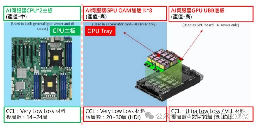 🟣 The global PCB market value is expected to increase to approximately $73.57 billion in 2024. Conventional or low-layer PCB products may face challenges of oversupply and homogenization competition. In the medium to long term, artificial intelligence, high-speed networks, automotive electronics (EV and ADAS), and portable smart consumer electronic devices with advanced AI functions are expected to drive incremental demand, becoming the most important growth drivers for the PCB market, prompting the industry to shift towards high value-added fields, with packaging substrates, HDI boards, and multilayer boards with more than 18 layers becoming the strongest growth segments.
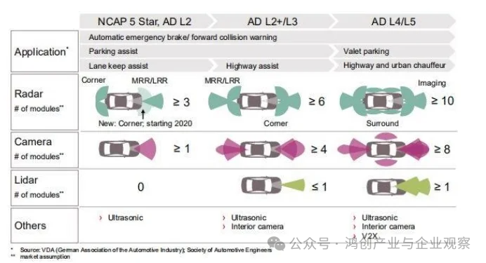 Reference: Prismark et al.
The End

Note: The above copyright belongs to the original author. This account maintains neutrality regarding the content of the article, only sharing more information, and does not represent the position of this account. If there is any infringement or omission, please contact us for correction or deletion. Thank you!
Editor: Li Dan
Reviewer: Wang Gang
Chongqing Electronic Circuit Manufacturing Industry Association
▼ Welcome to Submit Articles | Submission Method ▼
Association Email | [email protected]
Association Phone | 023—4623 1936 (Monday to Friday)
Association Address | 2nd Floor, Building 2, No. 12 Innovation Avenue, Changzhou Street, Rongchang District, Chongqing

Consultation

▼ Navigation Guide ▼