The ‘Pacemaker’ of Chip Manufacturing: RTP Crystals, the Next Breakthrough in Domestic Substitution!
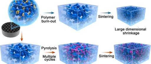
1. Overview of Industry Concepts RTP crystals specifically refer to the key components used in the rapid thermal annealing process—heaters/thermal field core materials. They do not refer to a single type of crystal material (such as quartz crystals), but rather a functional term that typically denotes ceramic or crystal materials capable of withstanding extremely high … Read more