1. Elon Musk announces the completion of the AI5 chip tape-out and the initiation of AI6 development;
2. ASML opens a technical academy in the U.S. to train 1,000 chip equipment engineers annually;
3. Samsung adds $1.9 billion to upgrade its U.S. factory, deepening its high-end manufacturing layout;
4. Nokia invests $4 billion to expand its AI network business in the U.S.

1. Elon Musk announces the completion of the AI5 chip tape-out and the initiation of AI6 development
Recently, Elon Musk announced that the AI5 chip developed by his company is nearing the completion of its tape-out work, while the development of the AI6 chip has officially begun. This news marks the company’s continued deepening and technological breakthroughs in the field of artificial intelligence chips.
It is reported that the company’s goal is to put a new artificial intelligence chip design into mass production every 12 months. This strategic plan demonstrates its ambition in the field of artificial intelligence hardware and a high emphasis on technological innovation. Musk also revealed that the expected production volume of the final chips will exceed the total of all other artificial intelligence chips, which, if achieved, will significantly change the competitive landscape of the global artificial intelligence chip market.
Looking back at the company’s chip development history, its investments and achievements in the field of artificial intelligence have repeatedly attracted industry attention. The imminent tape-out of the AI5 chip and the initiation of the AI6 chip development not only represent an important technological milestone but also indicate the company’s broad prospects in future artificial intelligence application scenarios.
It is worth mentioning that the company’s rapid iteration in chip development and large-scale production plans will further promote the popularization and application of artificial intelligence technology, bringing new development opportunities to various industries. As the AI5 and AI6 chips gradually come to fruition, market expectations for their performance and application effects are also rising.
In summary, the company’s continuous investment and innovation in the field of artificial intelligence chips not only showcase its strong capabilities in the high-tech field but also inject new vitality into the development of global artificial intelligence technology. In the future, with the mass production and widespread application of new chips, its leadership position in the field of artificial intelligence is expected to be further consolidated.

2. ASML opens a technical academy in the U.S. to train 1,000 chip equipment engineers annually
According to reports, Dutch lithography equipment giant ASML opened a technical academy in Phoenix, Arizona, on Thursday, aimed at training engineers to maintain and repair the company’s highly complex chip manufacturing equipment.
The academy is located just minutes from Phoenix Airport and is designed to train over 1,000 engineers annually, specifically responsible for the maintenance and technical service of ASML chip manufacturing equipment.
ASML’s decision to establish this academy is primarily due to the significant expansion of advanced chip manufacturing capacity in the U.S. Intel and TSMC have announced large-scale expansions of their wafer fabs in the Phoenix area; Samsung is also expanding its semiconductor factory near Austin, Texas; and memory chip manufacturer Micron has planned multi-billion dollar expansion projects in the U.S.
This training center is ASML’s first self-owned training facility in the U.S. in nearly 20 years. Previously, engineers had to travel to Asia or Europe for equipment maintenance training. The newly established academy is equipped with 14 classrooms and a clean room.
ASML Vice President Clayton Pacheco stated that the facility is capable of operating around the clock, and it is expected that the number of trained engineers will increase to 2,000 in the future.
Currently, engineers are already receiving training at this center. In addition to ASML’s own employees, other companies operating wafer fabs (i.e., chip manufacturing plants) can also pay ASML to provide professional training for their engineers.
According to Pacheco, the basic maintenance training cycle for engineers at ASML is 3 to 6 months; if it involves more complex equipment maintenance tasks, the training duration will be extended accordingly.

3. Samsung adds $1.9 billion to upgrade its U.S. factory, deepening its high-end manufacturing layout
According to reports, Samsung Electronics plans to invest approximately $1.9 billion to upgrade its semiconductor wafer fab in Austin, Texas, to enhance existing production lines and introduce cutting-edge chip manufacturing equipment. This move marks Samsung’s continued deepening of its high-end manufacturing capabilities in the U.S., particularly by strengthening its cooperation with tech giants like Apple and Tesla, consolidating its strategic position in the advanced semiconductor field.
It is reported that one of the core goals of this investment is to enhance the production capacity of CMOS image sensors (CIS). Industry news indicates that Samsung is jointly developing a 1/2.6-inch ultra-wide-angle image sensor with Apple, which is expected to be used in the iPhone 18 and subsequent models to be released in 2026. Although the specific technical parameters have not been publicly disclosed, if this collaboration proceeds smoothly, it means that Samsung will become an important supplier of high-end mobile phone image sensors for Apple, following Sony.
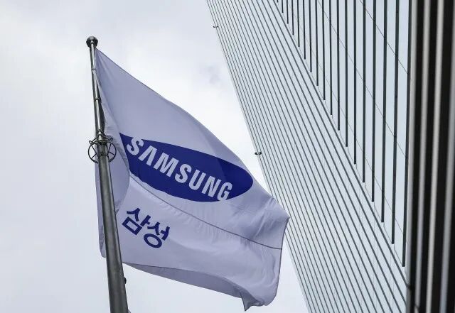
These custom sensors for Apple will be produced at the upgraded Austin factory, achieving a localized closed loop of “Made in America + American customers.” Additionally, this investment is expected to leverage more U.S. government policy benefits. The Austin City Council will vote on November 20 on a motion to include Samsung’s Austin factory in the “Texas Enterprise Project.” If approved, Samsung will be eligible for tax rebate incentives provided by the state government in the coming years.
Since the Austin factory began production in 1996, Samsung has invested over $40 billion, making it the largest single foreign investment project in Texas history. This additional investment of $1.9 billion will further drive the factory’s transformation from traditional logic chip manufacturing to high-value-added image sensors and advanced processes.
Furthermore, Samsung is building a new advanced process wafer fab in Taylor, focusing on the mass production of 2-nanometer chips, which is expected to officially start production in 2026. It is reported that this factory has secured a 2-nanometer foundry order for Tesla’s AI6 chip, which will become the manufacturing base for Tesla’s next-generation autonomous driving and AI computing core.

4. Nokia invests $4 billion to expand its AI network business in the U.S.
Nokia recently announced that it will invest $4 billion in the U.S. to expand its research and manufacturing business related to AI network connectivity. This plan is launched in cooperation with the administration of U.S. President Donald Trump, aiming to enhance the company’s ability to support secure and scalable AI-optimized networks.
According to Nokia’s statement, the new capacity will help improve productivity and expand the infrastructure needed to support next-generation connectivity technologies. This move comes as investors have renewed interest in Nokia’s AI plans, responding to the growing demand for advanced network equipment driven by the expansion of AI data centers and edge computing.
Nokia stated that this expenditure will enhance the supply chain of critical communication technologies in the U.S., further improving the company’s competitiveness in the global communications field. This investment not only marks Nokia’s strategic layout in the field of artificial intelligence but also reflects its emphasis on the U.S. market.
Previously, Nokia had already made certain accumulations and layouts in AI and network technology, but this large-scale investment is undoubtedly an important leap for it in this field. As AI technology continues to develop and application scenarios expand, Nokia’s initiative is expected to bring new growth points.
It is worth mentioning that Nokia’s investment plan aligns with the U.S. government’s policy to promote the development of domestic technology industries. By strengthening cooperation with the government, Nokia can not only gain policy support but also better grasp market demand and technological trends, laying a solid foundation for its future development.
In summary, Nokia’s $4 billion investment plan in the U.S. is not only an enhancement of its own technological strength but also an important contribution to the development of global communication technology. As the project progresses, its influence and market performance are worth continuous attention.
Hot Topics:
1.Counterattack! Wingtech Technology appeals to the Dutch government2.The U.S. plans to restrict imports of Chinese chip equipment, discussing H200 exports to China3.Breaking News! Arm Technology’s strategic announcement shines at ICCAD 2025
4.300456, 60 million yuan acquisition!
5.SMIC: Undertaking a large number of urgent orders!
6.A petroleum listed company crosses over to acquire this chip enterprise!
7.New Kai Lai makes a comeback! Tops the list
8.U.S. equipment giants cut off supply to China! Targeting storage and mature chips


Follow! Share! Like together!↓↓↓