Overview of the Semiconductor Materials Industry
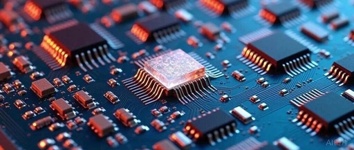
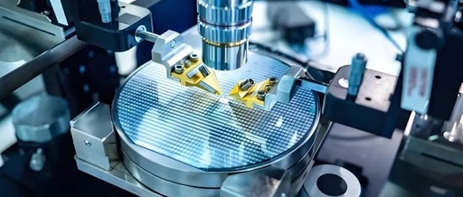
Overview Semiconductor materials can be categorized by application into wafer manufacturing materials (accounting for 63.6%) and packaging materials (36.4%), among which the core categories of wafer manufacturing materials include silicon wafers, electronic specialty gases, photoresists, and CMP materials, which are considered the “bottleneck” core categories. In terms of cost distribution among various materials, silicon wafers … Read more