Hello, everyone. Today, we will discuss thermal oxidation in chip manufacturing.
Oxides have various applications in the semiconductor industry:
- Isolation (interlayer dielectrics, etc.)
- Scattering oxide layers (ion implantation)
- Adapting layers (local oxidation of silicon, etc.)
- Flattening (edge rounding, etc.)
- Mask layers (diffusion, etc.)
- Alignment marks (photolithography)
- Cover layers (corrosion prevention, etc.)
- And more
When combined with silicon, oxides exist in the form of silicon dioxide (SiO₂). It can be deposited as a very thin, electrically stable, and uniform film.
Silicon dioxide (commonly referred to as silica) has strong corrosion resistance and can only be etched by hydrofluoric acid (HF). Water or other acids do not affect it, and due to the presence of metal ions, alkaline solutions (potassium hydroxide KOH, sodium hydroxide NaOH) cannot be used. In contrast, both potassium hydroxide and sodium hydroxide are important reagents for anisotropic wet etching in micromechanics. The chemical reaction of silicon dioxide with hydrofluoric acid is as follows:

Additionally, oxide layers are suitable for integrated circuits because they can meet electrical requirements (such as gate oxide layers, interlayer dielectrics, field oxide layers).
Thermal Oxidation
Silicon wafers undergo oxidation treatment in a furnace at approximately 1000℃. The furnace contains a quartz tube, and the silicon wafers are placed on a carrier made of quartz glass. The heating system has multiple heating zones, and the chemical supply is achieved through multiple pipelines. Quartz glass has a very high melting point (over 1500℃), making it suitable for high-temperature processes. To avoid cracking or warping of the quartz tube, the temperature must be increased slowly (for example, 10℃ per minute), and high-precision temperature control of the furnace tube can be achieved through independent heating zones.
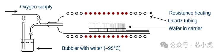
Oxygen is introduced in gaseous form and reacts with the surface of the silicon wafer to generate silicon dioxide, ultimately forming an amorphous glass-like thin film. Depending on the gases used, various types of oxidation reactions can occur (thermal oxidation must be performed on bare silicon surfaces).
Thermal oxidation can be divided into dry oxidation and wet oxidation, with wet oxidation further divided into traditional wet oxidation and hydrogen peroxide combustion oxidation.
1. Dry Oxidation
Dry oxidation is conducted in a pure oxygen atmosphere, where silicon reacts with oxygen to produce silicon dioxide.
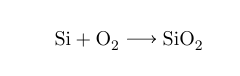
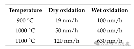
The actual operating temperature for this process is between 1000 and 1200℃. If a very thin and stable oxide layer is required, a lower temperature (around 800℃) can be used.
Characteristics of Dry Oxidation:
-
Slow growth rate of the oxide layer
-
High density
-
High breakdown voltage
2. Wet Oxidation
In wet thermal oxidation, oxygen flows through a bubbler containing hot water (approximately 95℃). Therefore, in addition to oxygen, there will also be moisture in the form of water vapor inside the quartz tube, and the oxidation reaction is as follows:
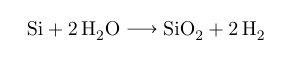
The operating temperature for this process is between 900 and 1000℃.
Characteristics of Wet Oxidation:
-
Can grow quickly at low temperatures
-
Quality is lower than that of dry oxide layers
3. Hydrogen Peroxide (H2O2) Combustion Oxidation
In the hydrogen peroxide combustion oxidation process, pure hydrogen gas is added to the oxygen. After both gases are introduced into the quartz tube, they combust in a low-temperature environment above 500℃ to avoid explosive gas reactions.
This process can produce oxide films with fast growth rates and low impurity content, capable of producing thick oxide layers and thin oxide films at moderate temperatures (900℃). The low-temperature characteristics also make it suitable for the preparation of doped silicon wafers.
Among all thermal oxidation processes, the growth rate of oxide layers on (111) crystal orientation substrates is higher than that on (100) crystal orientation substrates. Additionally, the dopants in the substrate can significantly increase the growth rate of the oxide layer.
Explanation of the Oxidation Process
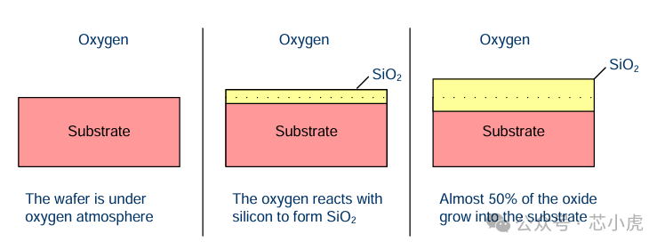
In the initial stage, oxygen reacts with silicon to generate silicon dioxide. Subsequently, the following oxygen atoms must penetrate the already formed oxide layer, diffuse to the underlying silicon crystal, and react with it.
Therefore, the growth rate in the early stages of oxidation mainly depends on the reaction time between oxygen and silicon, while once the oxide layer reaches a certain thickness, the growth rate is primarily determined by the diffusion speed of oxygen atoms through silicon dioxide. As the thickness of silicon dioxide increases, the growth rate gradually decreases.
Since the oxide layer has an amorphous structure, the chemical bonds inside are not fully saturated. There will be some dangling bonds (free electrons and holes) at the interface between silicon and silicon dioxide, forming a slightly positively charged region. These charges can adversely affect integrated circuits, so measures need to be taken to reduce charge accumulation.
This can be achieved by increasing the temperature during the oxidation process or by using wet oxidation processes that generate only a small amount of charge. Of course, wet oxidation and dry oxidation cannot be arbitrarily replaced— for example, the electrical performance requirements of gate oxide layers can only be met by oxide layers grown through dry processes.
Segregation Phenomenon
During the thermal oxidation of silicon, silicon reacts with oxygen to generate silicon dioxide. The thickness ratio of the generated oxide layer to the consumed silicon is 2.27, which means that silicon dioxide will grow into the silicon substrate, with the growth depth accounting for 45% of the total thickness of the oxide layer.
Dopants present in the substrate may either enrich in the oxide layer or in the silicon, depending on the solubility of the dopants—some dopants have higher solubility in silicon (e.g., phosphorus), while others have higher solubility in silicon dioxide (e.g., boron). This behavior can be calculated as follows, where k is the segregation coefficient:
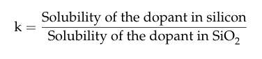
If k is greater than 1, the dopant will enrich at the substrate surface; if k is less than 1, the dopant will enrich in silicon dioxide.
If you have any comments or suggestions, feel free to leave a message or send a private message. If there are any inaccuracies, please feel free to point them out. The editor is also learning and growing.


*Disclaimer:This article is created by the original author. The content of the article reflects their personal views, and our reposting is solely for sharing and discussion, not representing our endorsement or agreement. If there are any objections or copyright issues, please contact us for removal! Source: “Semiconductor Technology”
▌⊰Related Knowledge Navigation ⊱
Process flow diagram of CMOS in semiconductor manufacturing
What is Q-Time in smart manufacturing?
How to understand Process Flow in semiconductor smart manufacturing
What stages must a semiconductor chip manufacturing FAB go through to achieve full automation?
In batch operations, when does a semiconductor FAB use Lot? When does it use Batch?
▌Click on “Chip Little Tiger” below ↓ to follow me, click the upper right “set as a star” to share more chip knowledge and news
▌If you like it, please “like” + “look” ✿, thank you
▌For learning, communication, and collaboration, please scan the following to add, please note your name + position + company, thank you!

▌Semiconductor industry information database, dedicated to those in need, thank you!