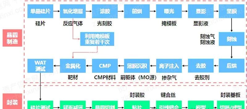
#04Equipment and Materials4.1 Key Equipment
- Photolithography Machine: As the core equipment in the fabrication process, its precision and stability have a decisive impact on the quality of chip pattern transfer. Modern photolithography machines utilize advanced optical systems and precise mechanical structures to project layout patterns onto silicon wafers with extremely high resolution, enabling the accurate delineation of fine patterns. Photolithography machines are also equipped with advanced alignment systems to ensure that each exposure aligns accurately with existing patterns on the silicon wafer, guaranteeing the accuracy and consistency of the chip structure.
- Etching Equipment: During the fabrication process, etching equipment removes specific materials from the surface of the silicon wafer through chemical or physical methods, forming the required grooves, holes, or microstructures. The performance of etching equipment directly affects the dimensional accuracy and surface roughness of the chip, which in turn impacts the electrical performance and reliability of the chip. When selecting etching equipment, factors such as etching rate, selectivity, uniformity, and the degree of damage to the silicon wafer surface must be carefully considered.
- Deposition Equipment: This is the key equipment used to deposit various thin film materials on the surface of silicon wafers. These thin film materials include metals, oxides, nitrides, etc., which play an important role in constructing the internal structure of the chip and achieving specific functions. The performance of deposition equipment directly affects the composition, structure, thickness, and uniformity of the thin film materials, thereby influencing the performance and stability of the chip. When selecting deposition equipment, factors such as deposition rate, composition control, thickness uniformity, and process stability must be considered.
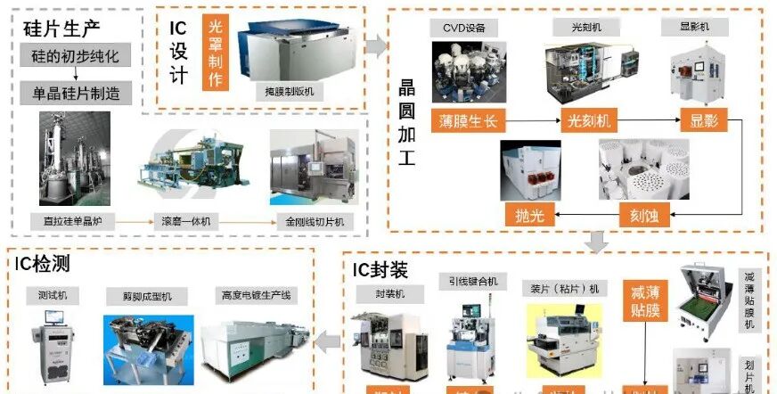 4.2 Material Usage
The selection and use of materials during the chip fabrication process is a crucial step.
- Photoresist: As one of the core materials in chip manufacturing, its performance directly relates to the precision and resolution of pattern transfer. High-quality photoresist should have good photosensitivity, adhesion, and corrosion resistance to ensure that the desired pattern mask can be accurately formed during the photolithography process. Additionally, the removal of photoresist must also be precisely controlled to avoid damage or residue on the silicon wafer surface.
- Etching Gases: Play a key role in removing excess material and forming fine structures during chip fabrication. Different etching gases have selectivity for different materials, so it is necessary to choose the appropriate etching gas based on actual needs. Furthermore, parameters such as temperature, pressure, and time during the etching process must be precisely controlled to ensure uniformity and accuracy of the etching.
- Thin Film Materials: Play an important role in constructing the internal circuits and interconnect structures of the chip. The deposition of thin film materials such as metals and oxides requires precise control over parameters such as thickness, uniformity, and purity to ensure the stability of circuit connections and signal transmission within the chip. Additionally, the properties and stability of thin film materials directly affect the reliability and lifespan of the chip.
| Semiconductor MaterialsSubdivided Materials | Main Uses | Main Application Stages | Development Trends | |
| Manufacturing Materials | Silicon Wafers | Over 95% of semiconductor chips and devices globally use silicon wafers as substrates | Throughout the manufacturing stages | Development of various silicon wafer technologies |
| Photoresist and Supporting Reagents | Used for developing, etching, etc., to transfer fine patterns from masks to the substrate to be processed | Developing, etching | Improved photolithography resolution, with KrF, ArF, and EUV becoming mainstream. | |
| Electronic Gases | Thin films, etching, doping, vapor deposition, diffusion, etc. | Thin films, etching, doping, vapor deposition, diffusion | Continuously shrinking line widths increase the purity requirements for electronic gases. | |
| Sputtering Targets | Semiconductor sputtering thin film deposition | Thin film deposition | Copper and tantalum targets are gradually replacing aluminum and titanium targets due to the increased weight of 12-inch wafers. | |
| High-Purity Reagents | Cleaning and etching of chips | Cleaning, etching | Grade requirements have risen from G3, G4 to G4, G5. | |
| CMP | IC silicon wafer polishing | Chemical mechanical polishing | The number of CMP polishing steps increases as chip sizes decrease. | |
| Photomasks | High-precision tools used for transferring “negatives” | Photolithography | Refinement and enlargement of masks. | |
| Packaging Materials | Packaging substrates | Mainly serve to fix, support, dissipate heat, and connect to lower circuit boards | Die bonding, reconstituted wafers, cutting/forming | Advanced packaging will gradually surpass traditional packaging, becoming mainstream.Packaging substrates have gradually replaced traditional lead frames as the mainstream packaging.Packaging substrates are developing towards higher density. |
| Lead Frames | Support chips and external lead pins, connecting chip solder points and lead frames or substrates | Die bonding, wire bonding | ||
| Bonding Wires | Connect chip solder points and lead frames or substrates to achieve electrical connection with external circuits | Wire bonding | ||
| Plastic Encapsulation Materials | Seal and protect the chip and lead frame | Plastic encapsulation | ||
| Chip Adhesive Materials | Materials that connect the chip to the carrier to fix the chip | Die bonding, plastic encapsulation |
#05Challenges and Solutions in Chip Fabrication
5.1 Design and Cost Challenges
- Design Complexity: The increase in the length and density of interconnects has made design and verification more complex.
- Process Technology Advancements: High precision requirements have driven a technological leap from deep submicron to nanoscale processes. This raises higher demands for equipment precision and material performance, leading to increased equipment costs and difficulties in material research, development, and procurement. Additionally, high-precision processes require stricter quality control to ensure the stability and reliability of each production stage, further increasing the overall cost of fabrication.
- Countermeasures:
- Design Phase: By introducing more efficient design tools and methods, such as high-level synthesis and automated routing, design efficiency can be improved and human errors reduced. Employing hierarchical and modular design concepts can decompose complex systems into more manageable sub-modules, thereby reducing design complexity.
- Cost Control: Optimizing process parameters and material selection is key. In-depth research into process principles and material performance can help find more cost-effective process solutions and material combinations. Increasing equipment utilization and reducing waste rates are also effective ways to lower costs. Strengthening communication and collaboration with supply chain partners ensures the stability of material supply and reasonable pricing.
5.2 Countermeasures for Fabrication Failures
- Strengthening Design Verification and Testing: Conducting thorough and rigorous simulation tests during the design phase, as well as strict layout verification and timing analysis before actual fabrication, can help identify and correct potential issues as early as possible, significantly improving the success rate of fabrication.
- Tight Communication with Fabrication Vendors: Various process and equipment issues may arise during fabrication, so establishing a regular communication mechanism with fabrication vendors to provide timely feedback and resolve issues is crucial for ensuring smooth fabrication.
- Establishing a Comprehensive Failure Analysis and Improvement Mechanism: Even with thorough preventive measures and preparations, the possibility of fabrication failure still exists. By conducting in-depth analyses of the causes of failures, the root problems can be identified, and design and fabrication processes can be optimized to prevent similar issues from occurring again.
Disclaimer: Some articles in this public account are reprinted or adapted from the internet, and the copyright belongs to the original authors. However, due to the large number of reprints, it is impossible to confirm the true original authors, hence the source is indicated. If there are any copyright issues, please contact us for deletion! 【Cooperation and Consultation】 Please scan the QR code to add staff WeChat (please note the company name)
Click the card below to follow us