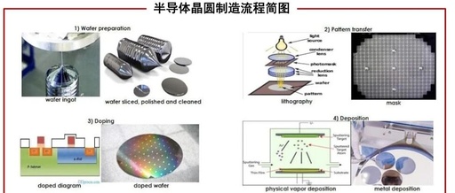
How Are Billions of Transistors Packed Inside Chips?

How Are Billions of Transistors Packed Inside Chips?

Chips are hidden in theelectronic devices that can be seen everywhere in cities, and smartphones, computers, and home appliances all rely on their control. The tiny chipintegrates a vast scale of circuits. When magnifying the chip, you can see that its interior is filled with densely packed circuit layouts, resembling a tightly woven highway, as … Read more

Why Are Chip Taping Costs So High?

Why Are Chip Taping Costs So High?

Click the blue text to follow us In the NHK documentary “The Story of the Electronic Nation,” a senior engineer mentioned: “During the two to three months leading up to each chip tapeout, I was filled with anxiety and couldn’t sleep. I constantly worried about what might go wrong… When the chip finally arrived and … Read more

What Is Chip Tape-Out (Part Two)

What Is Chip Tape-Out (Part Two)

Click the Blue Words Follow Us #03 Detailed Explanation of Chip Tape-Out Technology 3.1 Design Check and Layout Verification Before proceeding with chip tape-out, design checks and layout verification are essential steps that are crucial for ensuring the success of the tape-out. Design Rule Check (DRC):The main purpose of this process is to thoroughly review … Read more

What Is Chip Fabrication (Part Three)

What Is Chip Fabrication (Part Three)

Click the Blue Text Follow Us #04 Equipment and Materials 4.1 Key Equipment Photolithography Machine: As the core equipment in the fabrication process, its accuracy and stability have a decisive impact on the quality of the chip pattern transfer. Modern photolithography machines use advanced optical systems and precise mechanical structures to project layout patterns onto … Read more

Why Are Chip Tape-Out Costs So High?

Why Are Chip Tape-Out Costs So High?

Included in the collection #Li Chengguang61 #Tape-Out1 The chip industry is no stranger to tape-out. Tape-out refers to the process of manufacturing chips through a series of steps like an assembly line. This stage is a crucial link between chip design and mass production. In simple terms, it means handing over the designed scheme to … Read more

What Are the Eight Major Processes in Semiconductor Manufacturing?

What Are the Eight Major Processes in Semiconductor Manufacturing?

Are you familiar with the eight major processes in semiconductor manufacturing? 1. Wafer Processing Refining sand into single crystal silicon wafers. 2. Wafer Oxidation Forming a protective film on the wafer through thermal oxidation or chemical vapor deposition. 3. Photolithography Printing circuit patterns onto the wafer through coating, exposure, and development. 4. Etching After the … Read more

Detailed Explanation of Chip Tape Out: The Life and Death Leap of Hundreds of Millions of Transistors — The Ultimate Game from Design to Mass Production

Detailed Explanation of Chip Tape Out: The Life and Death Leap of Hundreds of Millions of Transistors -- The Ultimate Game from Design to Mass Production

Chip tape out (Tape Out) is the core step in transforming integrated circuit design into physical chips, involving design verification, process manufacturing, and sample testing, which directly determines the success rate of chip mass production. The name originates from the early tradition of “streaming” design drawings to magnetic tapes, which has now evolved into the … Read more

August 13 Technology Sector: Optical Modules and Semiconductors Join Forces to Open a New Chapter of Growth

August 13 Technology Sector: Optical Modules and Semiconductors Join Forces to Open a New Chapter of Growth

In the ongoing wave of technological advancement, the technology sector on August 13, 2025, once again became the market focus. Multiple fields are showing strong development momentum, bringing numerous surprises and opportunities for investors and technology enthusiasts. On that day, the A-share technology sector saw a pleasing increase. As of 11:28 AM, the communication equipment … Read more

From 0 to 1: A Detailed Breakdown of the SAW Wafer Fabrication Process (Part 1 – Photolithography)

From 0 to 1: A Detailed Breakdown of the SAW Wafer Fabrication Process (Part 1 - Photolithography)

[Image] The darling of the era under US-China trade relations, September 14, 2020, late at night, Hsinchu, Taiwan. TSMC’s factory is brightly lit, and the machines on the production line are still running at high speed, but there is an unusual tension in the air. Just a few hours ago, the U.S. Department of Commerce … Read more

The History of Chips

The History of Chips

Hello everyone, I am Yan Xiaobei, a science and engineering guy who understands a bit about economics.~ I am starting a new series to discuss some interesting stories in the chip field. In the first article, I talked about the origin of photolithography technology,the very first photolithography machine was actually modified from a microscope! The … Read more