Reading Good Books Together
From a pile of sand to a precision chip, what processes are involved, and what technologies are required at each stage?
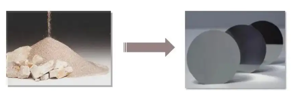
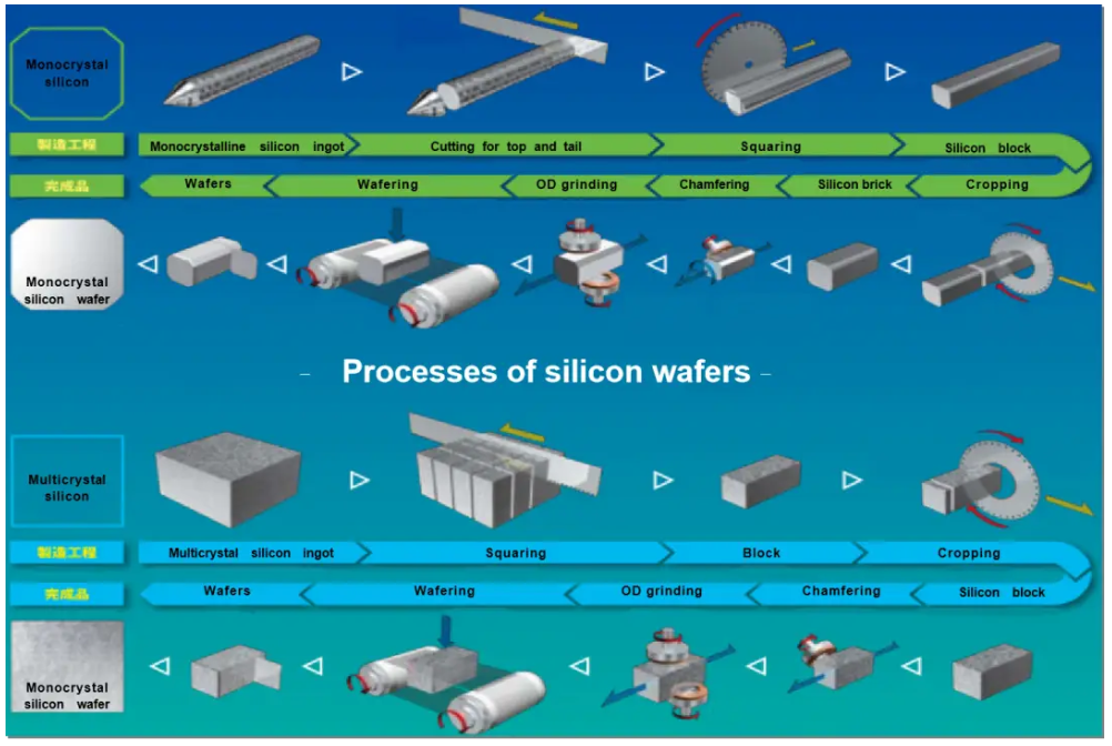
1. From Sand to Silicon Wafer.
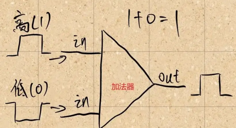
The term “semiconductor” refers to materials that have electrical conductivity between that of conductors and insulators. Conductors, such as iron, copper, and silver, can conduct electricity, while insulators, like rubber, cannot. Why are semiconductors used in chip manufacturing? Because the conductivity of semiconductors is related to the direction of the applied electric field, meaning their conductivity can be directional. For example, applying a positive voltage across a semiconductor may allow it to conduct; conversely, reversing the polarity of the voltage may prevent conduction. This property can be utilized to create “electronic switches.” We have all heard that “computers perform binary operations of 0 and 1”; this operation, at the physical level, refers to the “changes in high and low potential,” where high potential represents 1 and low potential represents 0. The changes in high and low potential can achieve complex transformations under intricate circuit designs, making it appear as if the computer is performing 0-1 operations. The electrical characteristics of semiconductors can be designed to create electronic switches, effectively realizing the transformation between high and low potentials.
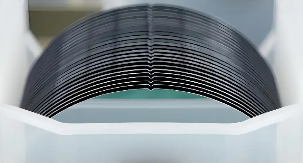
In nature, the least expensive semiconductor to obtain is silicon. The extraction of silicon material involves melting sand. At this point, some may think, “Silicon wafers are also used in photovoltaic cells.” Indeed, the processes for producing chips and photovoltaic cells are very similar in the silicon wafer production stage, both requiring the melting of silicon followed by cutting, grinding, and other processes. Therefore, you may see some stocks in the photovoltaic industry chain also associated with semiconductor concepts, such as Gaoce Co., Ltd. The biggest difference between silicon used for chips and silicon used for photovoltaics lies in their purity. In terms of purity, photovoltaic monocrystalline silicon wafers require silicon content between 4N-6N (99.99%-99.9999%), while semiconductor monocrystalline silicon wafers require around 9N (99.9999999%)-11N (99.999999999%), with purity requirements at least 1000 times higher than that of photovoltaic monocrystalline silicon wafers. In terms of appearance, semiconductor silicon wafers require higher standards for surface flatness, smoothness, and cleanliness than photovoltaic silicon wafers.
In summary, the process from sand to silicon wafer involves melting, slicing, grinding, etching, and polishing, ultimately forming circular high-purity silicon wafers (known as wafers).
The main players in the silicon material field include TCL Zhonghuan, while the slicing field is primarily represented by Gaoce Co., Ltd., and the polishing field includes Huate Gas and Dinglong Co., Ltd.
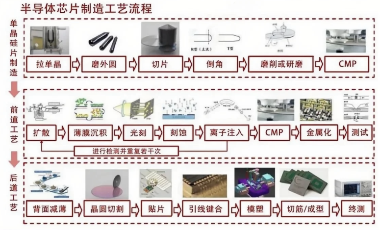
Now that you have obtained processed high-purity silicon wafers, the next step is to engrave circuits on the wafers to form usable chips. The following process can be roughly divided into front-end processes, back-end processes, and testing and packaging.
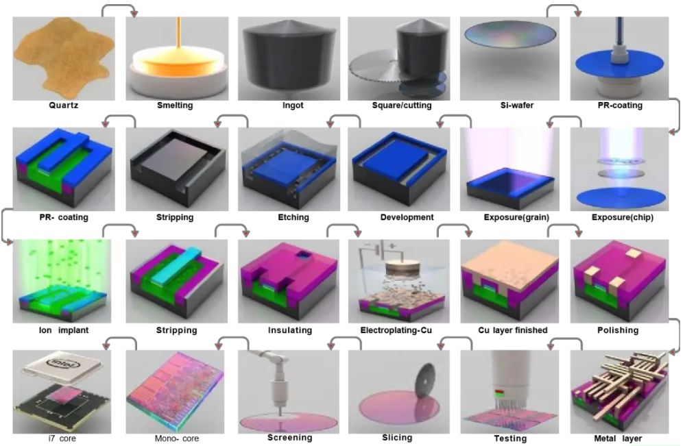
Manufacturing Phase One:Refining Silicon Ingots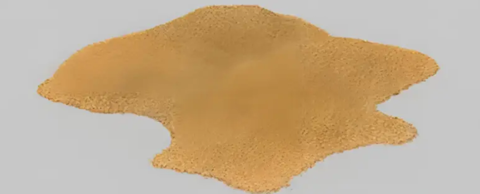 Sand: Silicon is the second most abundant element in the Earth’s crust, and deoxygenated sand (especially quartz) contains up to 25% silicon, existing in the form of silicon dioxide (SiO2), which is the foundation of the semiconductor manufacturing industry.Silicon Melting:12inches/300millimeter wafer level, and so on. Through multiple purification steps, silicon of semiconductor manufacturing quality is obtained, scientifically known as electronic-grade silicon (EGS), with an average of at most one impurity atom per million silicon atoms. This image shows how large crystals are obtained through silicon purification and melting, ultimately resulting in silicon ingots.(Ingot).

Monocrystalline Silicon Ingots: Generally cylindrical in shape, weighing about100kilograms, with silicon purity of99.9999%.
Manufacturing Phase Two:Silicon Ingot Cutting
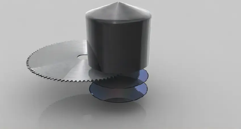
Silicon Ingot Cutting: Transversely cut into circular individual silicon wafers, which we commonly refer to as wafers.(Wafer).
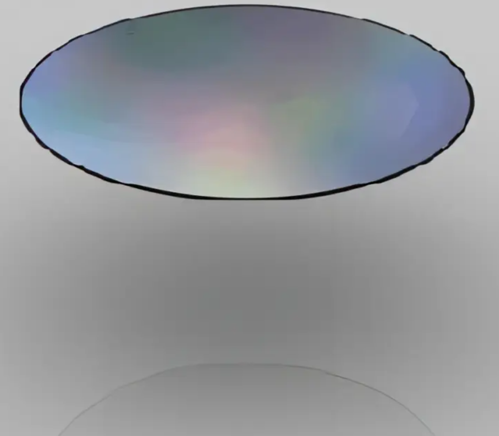
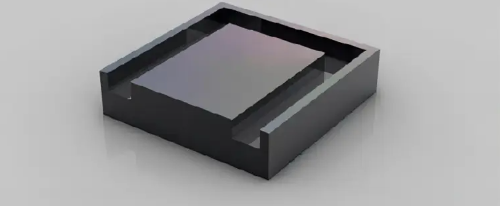
The wafer: The cut wafer becomes nearly flawless after polishing, with a surface that can even serve as a mirror. In fact, all chip companies do not produce these wafers themselves but purchase finished products directly from third-party semiconductor companies, then further process them using their own production lines, such as the currently mainstream45nm HKMG (High-K Metal Gate)..
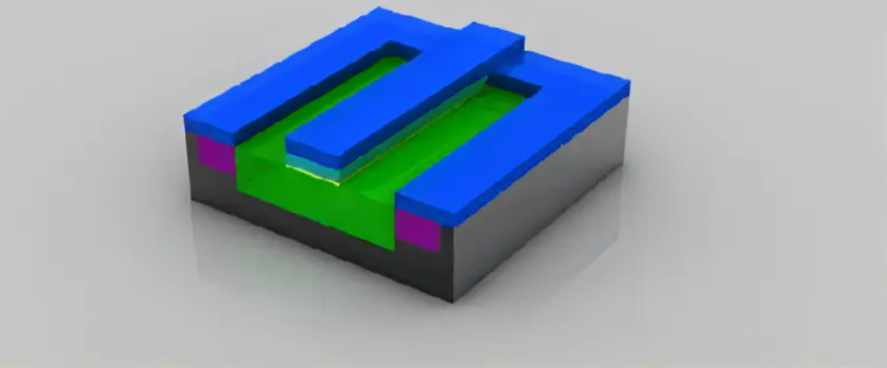
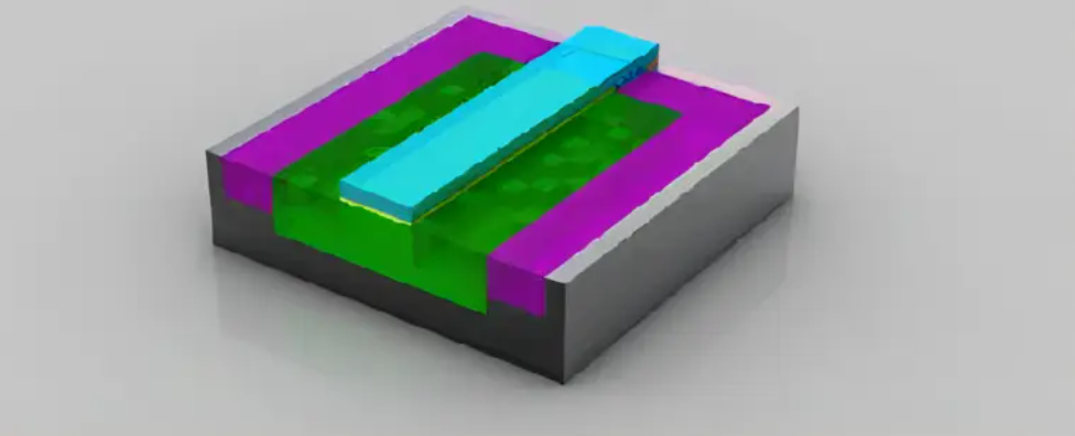
Manufacturing Phase Three:Photolithography

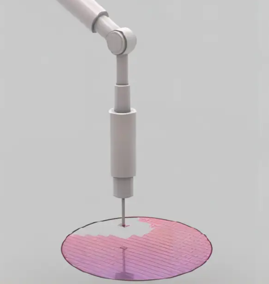
Photoresist:The blue part in the image is the photoresist liquid poured onto the wafer during its rotation, similar to the process of making traditional film. The rotation of the wafer allows the photoresist to be applied very thinly and evenly.
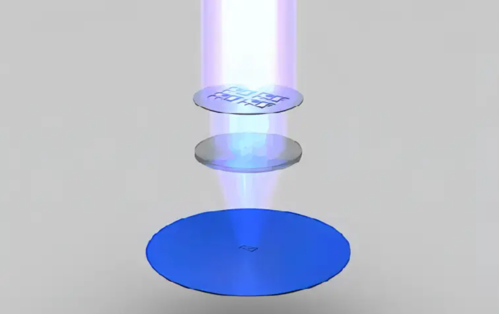
Photolithography: The photoresist layer is then exposed to ultraviolet light (UV) through a mask, becoming soluble. The chemical reaction that occurs is similar to the change in film when the shutter of a mechanical camera is pressed. The mask contains a pre-designed circuit pattern, and when ultraviolet light passes through it and hits the photoresist layer, it forms the circuit pattern for each layer of the microprocessor. Generally, the circuit pattern obtained on the wafer is one-fourth of the pattern on the mask.
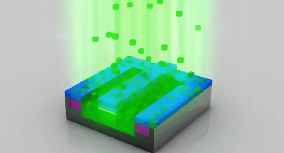
Photolithography: This leads to the level of transistors sized between 50-200 nanometers. A single wafer can yield hundreds of processors, but from here, we will narrow our focus to one of them to demonstrate how transistors and other components are made. Transistors act as switches, controlling the direction of current. Today’s transistors are so small that approximately30 millioncan fit on a needle tip.
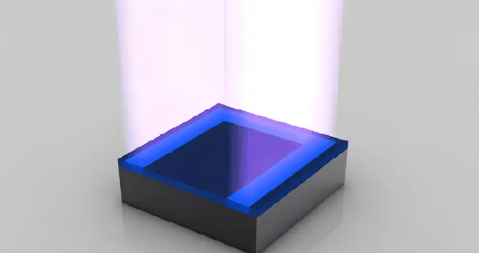
Manufacturing Phase Four:Mission of the Photoresist
Dissolving the Photoresist:During the photolithography process, the photoresist exposed to ultraviolet light is dissolved, leaving a pattern consistent with that on the mask.
Etching:Using chemicals to dissolve the exposed parts of the wafer, while the remaining photoresist protects the areas that should not be etched.
Removing the Photoresist:After etching is complete, the mission of the photoresist is declared finished, and once removed, the designed circuit pattern can be seen.
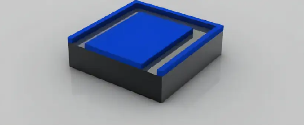
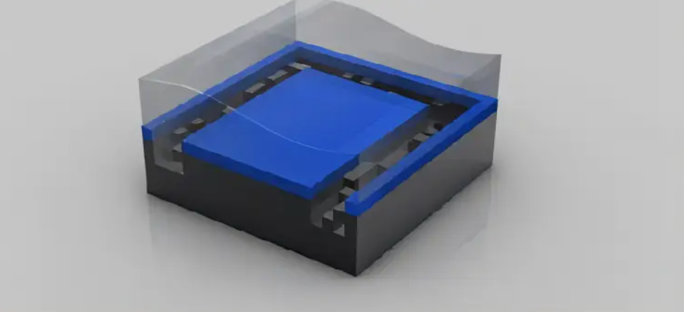
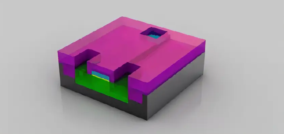
Manufacturing Phase Five:Ionic Implantation
Photoresist: Again, photoresist is poured(the blue part), then photolithography is performed, and the exposed parts are washed away, leaving the remaining photoresist to protect the areas that will not undergo ionic implantation.
Ionic Implantation:In a vacuum system, ions of the doped atoms are accelerated and irradiated(implanted)into the solid material, forming a special implanted layer in the injected area and altering the conductivity of the silicon in those regions. After being accelerated by an electric field, the speed of the injected ion flow can exceed300,000 kilometers per hour.
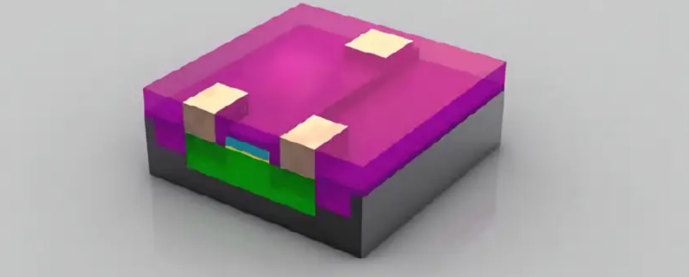
Removing the Photoresist: After ionic implantation is complete, the photoresist is also removed, and the implanted area(the green part)has been doped with different atoms. Note that the green color at this point is different from before.
Manufacturing Phase Six:Electroplating the Wafer
Transistor Ready: At this point, the transistor is nearly complete. Three holes are etched into the insulating material (shown in red) and filled with copper to interconnect with other transistors.
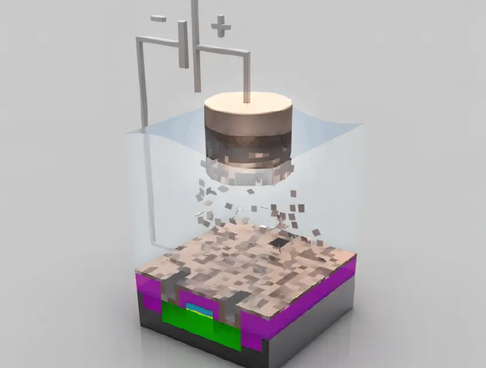
Electroplating: A layer of copper sulfate is electroplated onto the wafer, depositing copper ions onto the transistors. Copper ions move from the positive electrode (anode) to the negative electrode (cathode).
Copper Layer:After electroplating, copper ions deposit on the surface of the wafer, forming a thin copper layer.
Polishing:Excess copper is polished away, smoothing the surface of the wafer.
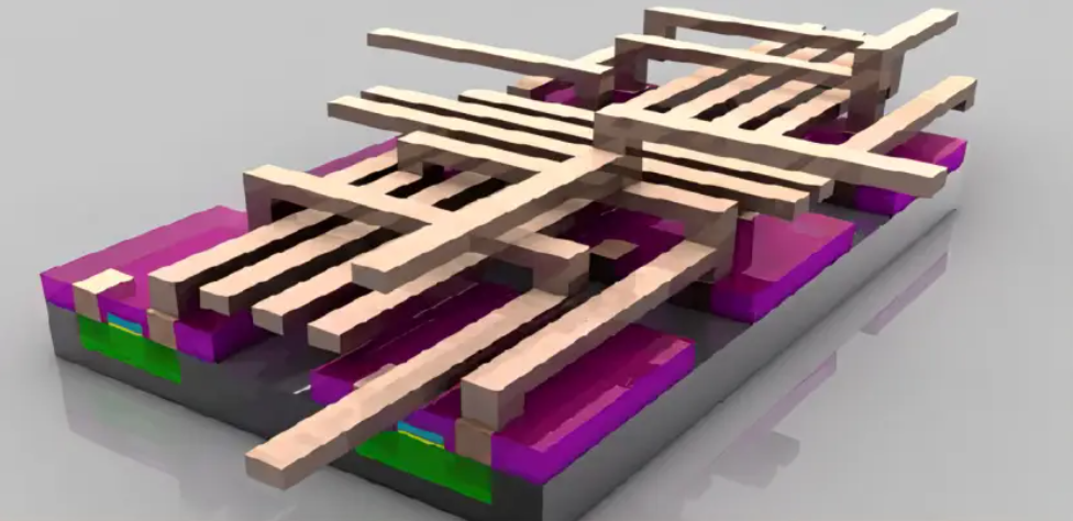
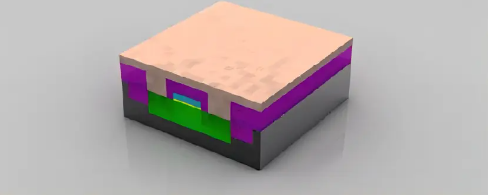
Metal Layer: At the transistor level, a combination of six transistors, approximately500nanometers. A composite interconnect metal layer is formed between different transistors, with the specific layout depending on the different functionalities required by the respective processors. The surface of the chip appears exceptionally smooth, but in reality, it may contain more than20layers of complex circuits, which, when magnified, reveal an extremely intricate circuit network resembling a futuristic multilayer highway system.
Manufacturing Phase Seven:Wafer Testing
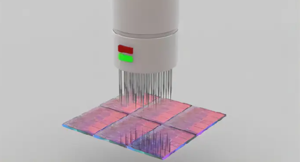
Wafer Testing: At the core level, approximately10millimeters/0.5inches. The image shows a partial view of the wafer undergoing its first functional test, comparing it with reference circuit patterns for each chip.
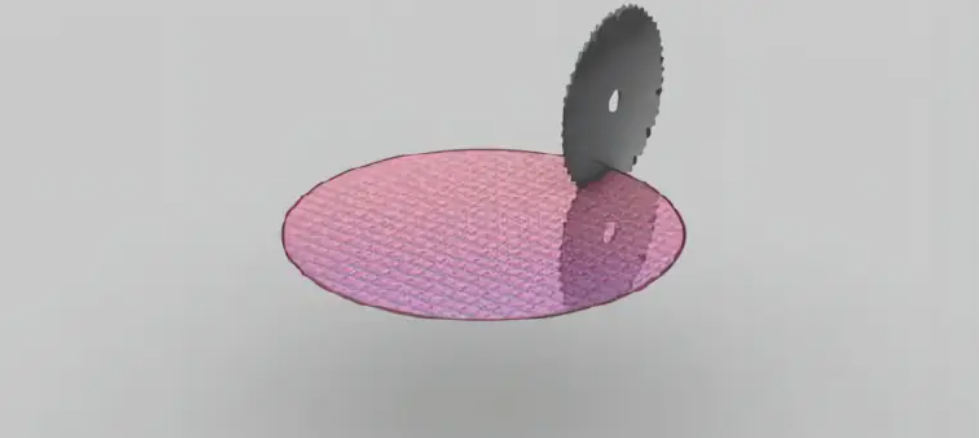
Wafer Slicing:(Slicing): At the wafer level,300millimeters/12inches. The wafer is sliced into pieces, each piece being the core of a chip(Die)..
Manufacturing Phase Eight::Wafer Inspection
Discarding Defective Cores:At the wafer level.Defective cores discovered during testing are discarded, leaving only the intact ones.
References can be found in the detailed document.
Feel free to scan the QR code to add the editor on WeChat.

Scan to join the knowledge circle and receive public account materials.