
Have you discovered the options for “Share” and “Like”? Click here to check it out.
*
Preliminary Review
From 0 to 1: A Detailed Breakdown of the SAW Wafer Fabrication Process (Part 1 – Photolithography)
From 0 to 1: A Detailed Breakdown of the SAW Wafer Fabrication Process (Part 2 – Thin Film Etching)
The previous two parts provided a detailed introduction to the process route of SAW. In fact, almost every step of the wafer fabrication process relies on the participation of specialty gases and functional liquids. They play a supportive role in the process and are often overlooked because they are not physically manifested. However, their involvement gives life to the entire process, just as we cannot live without air and water.
The Art of Gases in SAW – Specialty Gases
The global industrial gas industry began in the late 18th century and has matured significantly. The foundational period (1900s-1940s): The low-temperature separation and purification revolution enabled large-scale separation of oxygen, nitrogen, and argon, forming the basis of the industrial gas industry. At this time, gas purity was only sufficient for welding and metallurgy, with metal impurity concentrations still reaching ppm levels, which could not meet semiconductor demands. Rapid development period (1950s~): In 1957, Air Products successfully mass-produced 5N grade (99.999%) ultra-pure hydrogen and nitrogen for Texas Instruments’ silicon transistor diffusion process, marking the true starting point for industrial gases in the semiconductor industry. The rise of the electronics industry drove the development of specialty gases, while increased consumption in traditional markets propelled the growth of the industrial gas sector, laying the foundation for semiconductor industry development. To this day, specialty gases still occupy a large market share abroad, as shown in Figure 32.
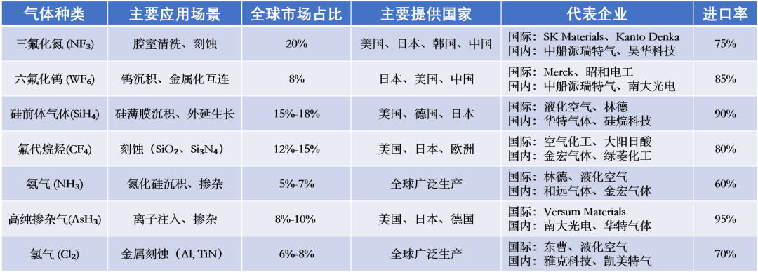
Figure 32 Market Share of Major Gases in Semiconductors
In the SAW process, specialty gases are mainly concentrated in three areas: photolithography, sputtering, and etching.
As mentioned in the photolithography section, the reduction of the light source wavelength λ is the most important precision technology evolution direction for photolithography machines. Among the various types of lasers, gas lasers maintain an important position due to their relatively simple structure, excellent beam quality, and rich wavelength selection. In photolithography machines, specialty gases act as the “light source,” providing laser sources at corresponding wavelengths. Their core working principle relies on the particle number inversion between energy levels within specific gas media and the stimulated emission process. By forming different molecules in the laser, different wavelengths of laser can be released. For example, in KrF photolithography machines, fluorine (F), krypton (Kr), neon (Ne), and helium (He) each play different roles. After high-energy particle collisions generated by electron beams, Kr⁺ and F⁻ are ionized, and with the help of the buffer gas neon (Ne), collisions occur, allowing neon to carry away excess energy and momentum, thus forming excited KrF excimers. When the excited KrF excimer transitions to the ground state, it releases photons with a wavelength of 248nm. The extreme ultraviolet (EUV) light (13.5nm) is not directly produced by gases; it is generated by bombarding tiny tin droplets with high-power lasers (such as CO₂ lasers) to create high-temperature plasma, utilizing the highly ionized tin ions in the plasma to emit light. The essential difference is that in DUV, gases serve as the “fuel” for laser generation, while in EUV, gases are tools for environmental control, contamination protection, and debris removal.
Figure 33 Wavelengths of Photons Released by Different Molecules
Sputter deposition technology is one of the core processes in modern thin film preparation and plays a crucial role in many high-tech fields. The core of the sputtering process lies in using inert gas ions to bombard the surface of solid target materials, transferring momentum to sputter atoms or molecules from the target, which are ultimately deposited on the substrate to form thin films. In this precise “sculpting” process of physical vapor deposition, the selection, purity, and precise control of specialty gases are not merely environmental media; they fundamentally determine the characteristics of the sputtering plasma, the sputtering behavior of the target material, and the growth dynamics of the thin film. Parameters such as the type of specialty gas, partial pressure, and flow rate act like a conductor, precisely controlling every aspect of the sputtering process.
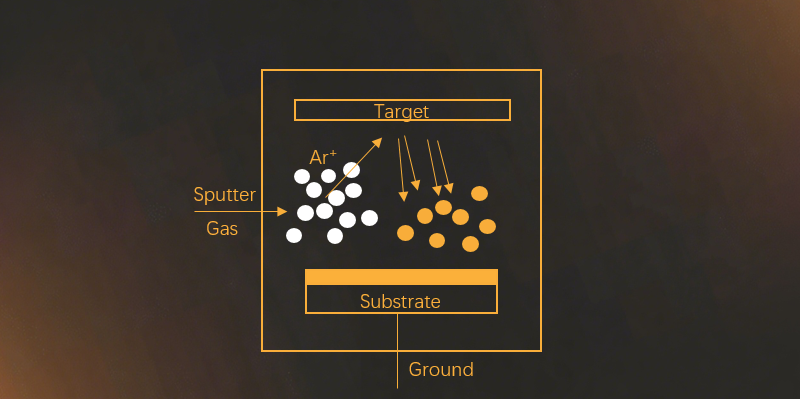
Figure 34 Sputtering Principle Diagram
In SAW, sputtering mainly uses argon (Ar), oxygen (O), and nitrogen (N) gases. In the preparation of metal films, argon is the primary sputtering gas, ionizing under high-pressure electric fields to form plasma, which then bombards the cathode metal target at high speed. This high-energy bombardment transfers kinetic energy to these atoms or molecules, causing them to exceed their binding energy and be sputtered away from the target, ultimately depositing metal atoms on the wafer to form a metal film layer. In the preparation of compound films, argon is also the main sputtering gas, but it is supplemented with reactive gases. For example, in the preparation of SiO₂ films, the cathode target material is silicon, and the reactive gas oxygen molecules are ionized into oxygen atoms in the plasma. These reactive oxygen particles chemically react with the sputtered Si atoms, depositing on the wafer to form SiO₂ film layers. Moreover, argon, with its high sputtering efficiency, absolute chemical inertness (ensuring target purity), stable and controllable plasma formation, and low cost, plays an irreplaceable role.
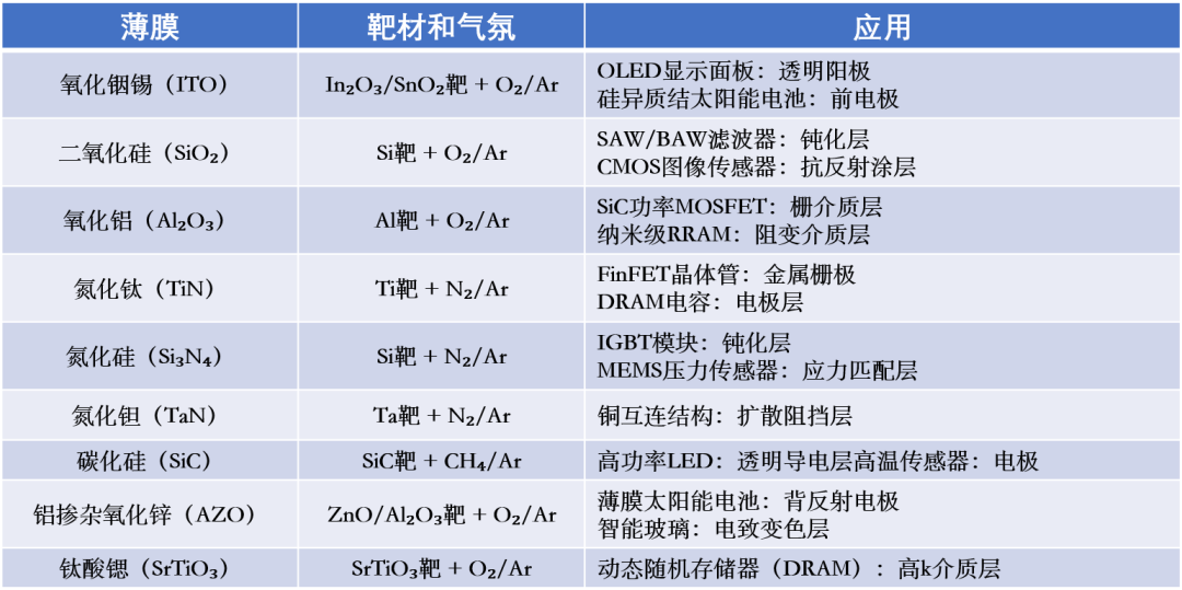
Figure 35 Synthesis of Different Films and Their Application Scenarios
In the microcosm of chips, etching gases play the role of “precision sculptors,” responsible for meticulously “carving” the blueprints drawn by photolithography into the underlying materials. The selection of specialty gases directly determines the precision, speed, and perfection of the final product.
Etching is divided into dielectric etching and metal etching. In dielectric etching, gases such as argon, oxygen, nitrogen, helium, sulfur hexafluoride, tetrafluoromethane, and trifluoromethane are mainly used. Fluorocarbon gases (CF₄, CHF₃) react with silicon-based dielectrics to generate volatile SiF₄ for etching, while sulfur hexafluoride (SF₆) serves as an auxiliary fluorine source, primarily used for silicon etching, with limited effects in dielectric etching. Argon (Ar) enhances physical sputtering through ion bombardment, breaking the passivation layer and improving anisotropy; oxygen (O₂) consumes excess carbon to suppress polymer deposition and increase etching rates; nitrogen (N₂) protects sidewalls and improves selectivity to SiO₂; helium (He) serves as a backflow gas for efficient heat conduction, preventing wafer overheating and process fluctuations. In short, the gas combination synergizes through chemical reactions (fluorine radical etching) and physical bombardment (Ar⁺), supplemented by passivation layer control (O₂/N₂/CHF₃) and thermal management (He).
Dry etching of metals is achieved through specific gases for precise corrosion, with core gases including chlorine (Cl₂), sulfur hexafluoride (SF₆), boron trichloride (BCl₃), methane (CH₄), oxygen (O₂), and argon (Ar). Chlorine is the primary etchant, and the chlorine radicals generated after plasma activation can react with metals like aluminum and titanium to form volatile chlorides, achieving directional etching; the fluorine radicals released by sulfur hexafluoride are specifically used for rapid etching of tungsten and titanium nitride. In the SAW wafer fabrication process, dry etching primarily targets the aluminum metal layer. During aluminum etching, boron trichloride (BCl₃) and methane (CH₄) can be added. BCl₃ dissociates in plasma to release Cl radicals and BCl₂⁺ ions, which react with the aluminum oxide layer in a reduction reaction, breaking down the oxide layer. Once the oxide layer is removed, the ionized Cl radicals can quickly react with the exposed aluminum metal, while CH₄ dissociates in plasma to generate CH₃ radicals, which react with the aluminum surface to form an Al-C polymer layer that effectively suppresses lateral corrosion. Overall, in the dry etching process of aluminum metal, BCl₃ acts as the vanguard to break through the outer oxide layer, Cl₂ serves as the main force to react with aluminum metal to form patterns, and CH₄ acts as the backup to protect the sidewalls. Oxygen plays a dual role in different processes: it enhances the etch resistance by hardening the photoresist during aluminum etching and catalyzes reactions to accelerate the generation of volatile products during molybdenum etching. Argon primarily serves as a dilution gas to adjust reaction concentrations while utilizing ion bombardment to break through the metal surface oxide layer, ensuring a smooth start to the etching process. These gases work synergistically to achieve high-precision processing of metal materials in a plasma environment. It can be said that without these tailor-made, precisely controlled specialty gases, the breathtaking nanoscale circuit structures in modern chips would remain a mere illusion. They are the “unsung heroes” of precision manufacturing in the microcosm and the “invisible engines” driving the continuous advancement of Moore’s Law!
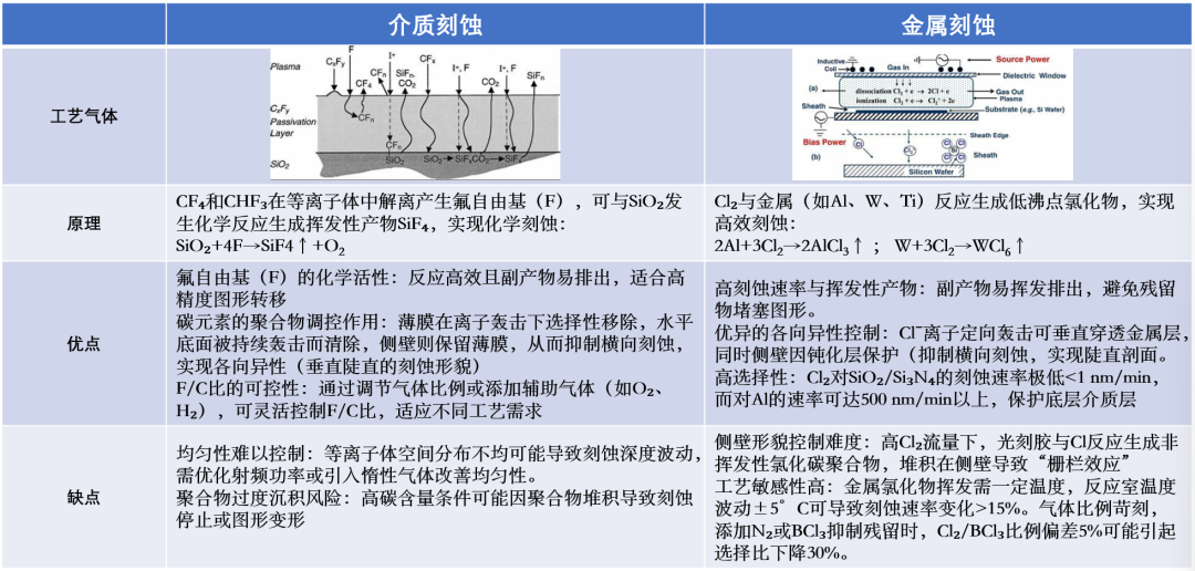
Figure 36 Dielectric Etching vs. Metal Etching
The Lifeblood of SAW – Functional Liquids
In semiconductor processes, functional liquids play a crucial role, spanning multiple key steps in wafer manufacturing. Their main functions include: cleaning, etching, developing, stripping, polishing, cooling, lubricating, dissolving, delivering chemical reactants, and forming thin films. These functional liquids are the indispensable “blood” of semiconductor manufacturing, and their performance and quality directly affect the final chip yield, performance, and reliability. The three main types closely related to the SAW wafer fabrication process are: cleaning solutions, developing solutions, and stripping solutions.
Cleaning solutions are the “invisible guardians” of chip manufacturing, ensuring chip yield and performance. The complex semiconductor manufacturing process involves dozens of layers, with cleaning processes accounting for over 30% of the total chip manufacturing steps. Cleaning before and after each step can block the transfer of contaminants, preventing defects from amplifying in subsequent stages and significantly improving overall yield. Cleaning not only ensures the wafer surface is clean, allowing for uniform photoresist coating and avoiding pattern distortion or resolution degradation, thus enhancing photolithography precision, but also effectively removes particles, metal ions, organic residues, and natural oxide layers from the wafer manufacturing process. Due to process upgrades, the demand for cleaning has surged; for example, a 90nm chip requires about 90 cleaning steps, while the 20nm node has increased to 215 steps, and the number of steps continues to rise for 14nm and below processes.
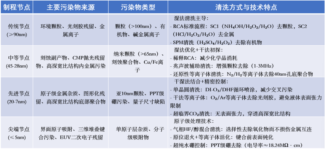
Figure 37 Sources of Contamination in Different Process Nodes
In the manufacturing of SAW filters, the cleaning steps are primarily concentrated in the early stages. The LT/LN wafers produced by material manufacturers undergo polishing treatment, which inevitably leads to the adhesion of some contaminant particles, organic substances, and some inorganic materials. The presence of impurities can cause abnormalities during the first photolithography coating, often resulting in comet-like tails that reduce photolithography yield.
Figure 38 Semiconductor Wafer Cleaning
Although material manufacturers perform cleaning actions before shipment, they cannot ensure that the cleanliness meets wafer fabrication requirements. Therefore, a unified cleaning of the wafer surface is necessary before photolithography, primarily achieved through the precise combination of acidic and alkaline solvents with oxidants to accomplish microscopic cleaning of the wafer surface. Based on chemical composition and function, they can be divided into acidic solutions – the “dissolvers” of metals and oxides; alkaline solutions – the “strippers” of particles and organic substances; and oxidants – the “incinerators” of contaminants.
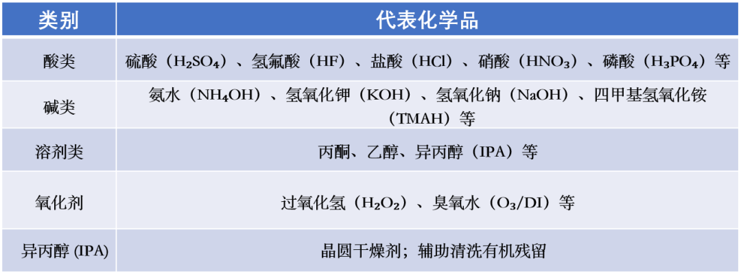
Figure 39 Classification of Chemicals in Semiconductor Cleaning
As previously mentioned, in the precise and complex manufacturing process of SAW filters, photolithography technology plays a key role in defining the core electrode patterns of devices. As a critical step in the photolithography process, the “developing” process and its core reagent – developing solution – have a decisive impact on the final performance of the devices. The role of the developing solution is to selectively dissolve the exposed area (positive photoresist) or unexposed area (negative photoresist) of the photoresist after exposure through precise and controllable chemical reactions, thereby transferring the fine circuit patterns from the mask onto the photoresist layer on the wafer surface. Therefore, the selection, formulation optimization, and process control of the developing solution directly relate to core parameters such as line width accuracy, edge steepness, and pattern fidelity of the SAW filter electrodes.
In early semiconductor photolithography processes, strongly alkaline aqueous solutions based on sodium hydroxide (NaOH) or potassium hydroxide (KOH) were primarily used as developing solutions. However, due to the sodium ions (Na⁺) and potassium ions (K⁺) they contain, which can cause fatal device contamination, they have gradually been phased out. Since the 1980s, tetramethylammonium hydroxide (TMAH) has gradually become the industry standard developer due to its excellent developing selectivity and low metal ion residue characteristics. Its typical working concentration is 2.38%, achieving micrometer-level patterning through the chemical reaction between the alkaline solution and photoresist. The technical focus during this stage was on purity control, with metal impurities needing to be below one billionth; otherwise, they could lead to circuit short circuits or leakage.
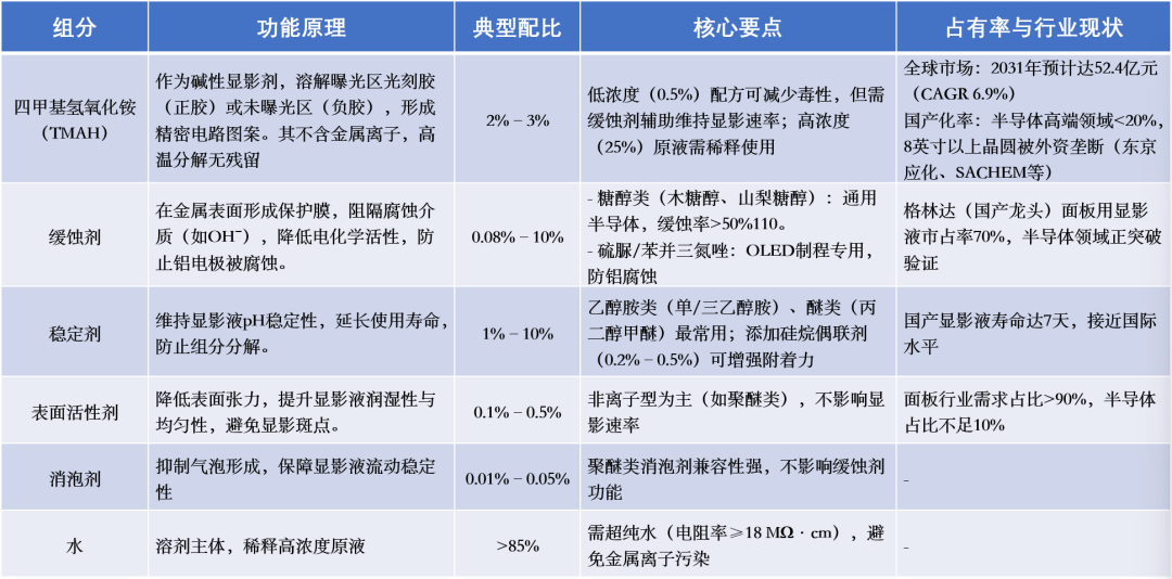
Figure 40 Main Formulation of Alkaline Developer TMAH
The development of TMAH developing solution has always revolved around two major themes: “smaller line widths” and “sustainability.” International giants (Tokyo Ohka Kogyo, SACHEM, etc.) still dominate 87% of the high-end market, but domestic companies are gradually breaking the technological blockade through breakthroughs in purity, capacity expansion, and policy support. Future innovations need to accelerate in EUV compatibility and closed-loop recycling to support the demand for domestic chip autonomy below the 3nm process.
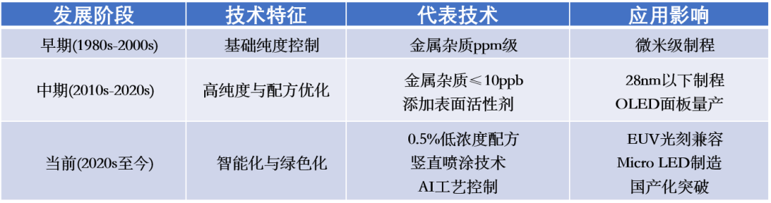
Figure 41 Key Technological Evolution of TMAH
In the high-precision manufacturing process of SAW filters, the lift-off process is a key step in defining the IDT electrode patterns. The functional liquids in the lift-off process mainly consist of NMP, deionized water, and IPA in processing order. As the core solvent of this process, NMP, with its excellent solubility and selectivity, undertakes the core mission of precisely stripping the photoresist mask and residues.
N-Methyl-2-pyrrolidone (NMP) is an efficient organic solvent that, due to its high boiling point and strong dipole moment, can disrupt the van der Waals forces and hydrogen bonds between the polymer chains of the photoresist. The carbonyl oxygen in its cyclic amide structure penetrates the polymer network through dipole-dipole interactions, causing the cross-linked resin to swell and dissociate, achieving over 90% removal rate of the photoresist in the lift-off process. NMP effectively dissolves the photoresist layer through penetration and swelling while ensuring zero chemical erosion on the LT/LN piezoelectric substrate, thus guaranteeing the edge steepness and pattern fidelity of the IDT electrodes in SAW manufacturing.
Deionized Water (DI Water) primarily serves to interrupt the lift-off reaction and remove residual NMP. NMP residues can continuously affect the IDT in subsequent processes, so deionized water is used to continuously dilute and rinse away NMP residues.
Isopropanol (IPA) plays a key role in the drying stage: its low surface tension and the high interfacial tension of water create a significant gradient, triggering the Marangoni effect, driving the liquid film to contract towards the IPA-rich area; in the vapor drying process, IPA vapor condenses on the wafer surface to form an azeotropic mixture, achieving residue-free dehydration by reducing the hydrogen bond density of water molecules, lowering the surface water contact angle to <5°, thus avoiding drying stain defects, while combined with thermal nitrogen processes, achieving higher efficiency.

Figure 42 Chemicals in the Lift-off Process
Comparative Analysis of SAW Filter Processes
The traditional surface acoustic wave (SAW) filter process is relatively simple and practical. The previous two parts have provided a preliminary introduction to its processes. However, to meet the demands of low temperature drift in communication systems, the TC-SAW process with a thick temperature compensation layer has emerged, as well as the FBAR process, which features high Q values: using thin film deposition and micromachining technology to form a suspended thin film structure on the substrate as a resonant cavity, along with the BAW process that meets high Q and high power demands: replacing the suspended layer of FBAR with stacked Bragg reflector layers. Due to space limitations, only the main characteristics of their process routes will be briefly summarized and compared here.
Characteristics of TC-SAW Process
Compared to the conventional NSAW process, the core of the TC-SAW (Temperature Compensated SAW) filter preparation process lies in the sputter deposition of a piezoelectric compensation layer with a negative temperature coefficient, typically AlN or SiO₂ (TCF≈-30ppm/°C), to offset the positive temperature coefficient of the conventional piezoelectric substrate (TCF≈45ppm/°C), thus achieving high stability of device frequency with temperature. SiO₂, with its mature temperature compensation capability and low cost, occupies over 95% of the TC-SAW temperature compensation layer market share. Although materials like AlN have theoretical advantages (high thermal conductivity and high sound speed), they are limited to specific high-end scenarios due to process compatibility and cost. The role of the piezoelectric compensation layer goes beyond this (taking SiO₂ as an example); even slight changes in SiO₂ can significantly alter the effective propagation speed of sound waves and the resonant frequency of the device. Precisely controlled SiO₂ layers help suppress certain unwanted lateral acoustic modes (noise), thereby improving the in-band ripple and out-of-band suppression characteristics of the filter. Based on this, the sputtering process plays an extremely critical role in TC-SAW manufacturing, primarily used for depositing temperature compensation layers, with core control requirements including:
1. Precise Stress Control: SiO₂ typically exhibits compressive stress. It is necessary to accurately adjust power, pressure, substrate temperature, and bias to match the stress with the IDT layer and align with design goals (often slight compressive stress). High accumulated stress can lead to wafer warping, cracking, or delamination.
2. Good Step Coverage: SiO₂ must uniformly cover the steep steps and grooves of the IDT. Poor coverage can lead to uneven local thickness, affecting compensation uniformity and potentially introducing parasitic modes. Applying bias can significantly improve thin film density, enhance adhesion, and control stress and step coverage.
3. Density and Insulation: Loose films contain more moisture/hydroxyl, leading to high acoustic loss, poor insulation, and poor temperature stability. Sputtered SiO₂ with bias is usually denser and contains less moisture than conventional SiO₂.
4. Clean Interface Quality: The SiO₂/IDT interface must be clean, steep, and free of reaction layers or contaminants to minimize acoustic loss and ensure stability.
5. Precise Thickness Control: Due to the low sound speed of SiO₂, a thicker compensation layer is required to achieve the same phase delay compensation. Thickness control typically employs CMP processes, Trim processes, or a combination of CMP and Trim processes, which is a key factor limiting the mass production of TC-SAW.
Characteristics of FBAR Process
In 1981, the Lakin team at the University of Southern California first proposed the suspended bulk acoustic wave resonator structure, laying the foundation for FBAR technology. Subsequently, in 1994, the Richard Ruby team at HP Labs (later Agilent/Avago) broke through the GHz frequency limit, developing an FBAR based on aluminum nitride (AlN) piezoelectric material, covering frequencies from 1.5 to 7.5GHz with a Q value exceeding 1000, solving the high-frequency communication compatibility issue. By 2001, Agilent (the predecessor of Avago) mass-produced the first FBAR duplexer (HPMD7901/7904) for the PCS1900MHz mobile phone band, marking FBAR’s official entry into the mobile communication market, which has now been around for 20 years.
As previously introduced, FBAR converts electrical signals into acoustic wave resonances through piezoelectric thin films (such as AlN), requiring the confinement of acoustic waves within micron-level structures to achieve total reflection. Its performance depends on the quality of the air cavity preparation. Compared to SAW, the process difficulty of FBAR is higher:
1. High Process Complexity: It requires constructing a vertically stacked thin film structure (bottom electrode/piezoelectric layer/top electrode), involving multiple layers of photolithography and etching, far exceeding the single photolithography process of SAW’s planar interdigital transducer (IDT);
2. Multiple Coating Steps with Stringent Precision: It requires multiple depositions of nanometer-level thin films (such as Mo electrodes/AlN piezoelectric layers), with thickness fluctuations needing to be controlled to <±1%, and the AlN piezoelectric layer requiring highly preferred crystal orientation (swing angle <2°); otherwise, the Q value drops sharply. Therefore, this part often employs sputtering or atomic layer deposition (ALD) for precise growth;
3. High Risk of Air Cavity Release: It requires etching sacrificial layers (such as SiO₂) through wet methods (such as HF solution) or dry methods (gas-phase HF). HF is highly toxic and can easily damage equipment, while also facing the risk of lateral etching leading to film collapse; after release, the micron-level suspended film can easily fail due to stress or capillary forces (stiction effect), requiring reliance on supercritical drying or support pillar structures for reinforcement; during the release process, care must be taken to avoid etching electrodes (such as Mo) or piezoelectric layers (AlN), as this may lead to frequency drift and performance degradation.
The “swimming pool” cavity structure in the FBAR process is the core of the technology, which has become a focus of research for various manufacturers. Currently, various types of process technologies have emerged, as shown in the table:
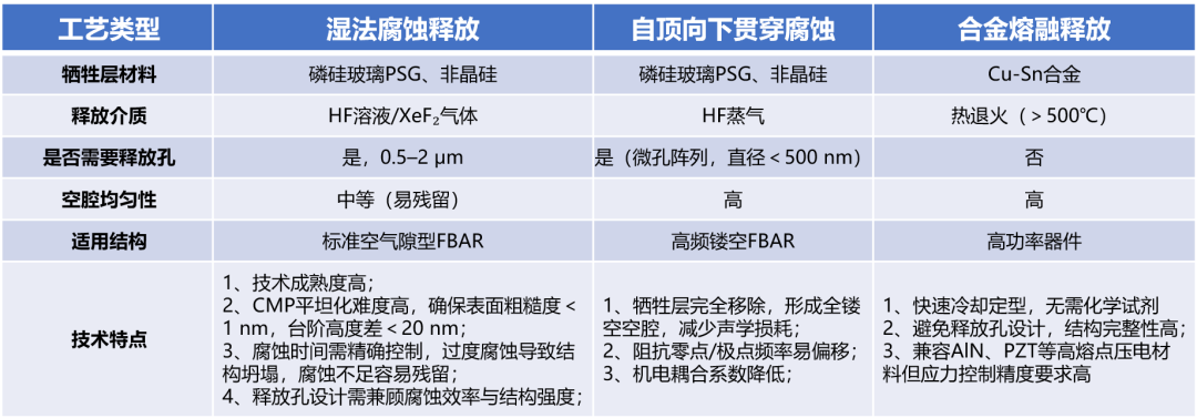
Figure 43 Types of FBAR Cavity Release Technologies
Characteristics of BAW Process
Due to the patents on FBAR’s swimming pool structure and its process shortcomings, the BAW filter was born. The BAW filter is theoretically a branch of FBAR, differing in that the air cavity is replaced with a Bragg reflector layer, while the remaining fabrication processes are basically similar. The Bragg reflector layer in the BAW filter is the core structure of the solid-state reflective resonator (SMR-type BAW), primarily functioning to achieve efficient reflection of acoustic waves through a strong contrast in acoustic impedance, effectively confining acoustic wave energy within the piezoelectric layer. The preparation of the Bragg reflector layer is a high-precision thin film deposition and patterning process, with core steps including:
1. First, the silicon or sapphire substrate is RCA cleaned to remove organic/metal contamination, followed by high-temperature annealing to release stress. Then, low acoustic impedance layers are deposited using PECVD, most commonly depositing λ/4 thickness of SiO₂ (good step coverage, relatively low temperature, moderate deposition rate, and good stress adjustability).
2. Then, a λ/4 thickness metal layer of tungsten/molybdenum is deposited using sputtering (high deposition rate, dense thin films, and good stress controllability).
3. This alternating stacking and CMP flattening is repeated for 3-7 pairs of high and low acoustic impedance layers, with CMP (chemical mechanical polishing) performed after each layer to ensure surface roughness <0.5nm.
4. To define the boundaries of the Bragg reflector layer, the stacked layers also need to undergo photolithography and etching, with the most common compromise being to pattern every 2-4 layers. If the last patterning is done all at once, while the process is simpler, it requires extremely high etching selectivity and sidewall morphology control.
From the above, it can be seen that the Bragg reflector layer involves alternating high-precision and high-stability PVD (sputtering) and PECVD processes, supplemented by precisely controllable photolithography and etching steps. The core is to achieve the stacking of numerous λ/4 thickness films while strictly controlling the stress, thickness uniformity, interface quality, surface roughness, and overall defect levels of each layer. The ultimate goal is to obtain a periodic structure with extremely high acoustic reflectivity, low loss, and mechanical stability at the target frequency, laying the foundation for high-performance SMR-BAW filters.
The above provides a basic introduction to the mainstream processes of the acoustic wave filter family. Below is a summary of their process characteristics in the table:
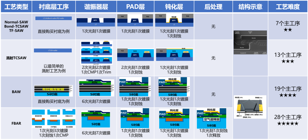
Figure 44 Comparison of Acoustic Wave Filter Process Routes
The Impact of Acoustic Wave Filter Processes on Design
In the design of SAW and FBAR filters, design and process are interdependent and mutually constraining: the design blueprint must be realized through the process, while the physical limits of the process define the feasible domain of the design. In addition to conventional design layout rules (Design Rule), the performance of the filter, especially the core operating frequency and the tuning degree of the resonator frequency during the simulation process, is fundamentally limited by the physical mechanisms of sound wave propagation and the characteristics of the processes.
The frequency of FBAR/BAW filters is determined by the propagation speed (𝑣) of sound waves in the piezoelectric layer and the structural thickness (𝑡), with the resonant frequency formula being: 𝑓=𝑣/2𝑡. Therefore, the design of the operating frequency is mainly achieved by adjusting the thickness of the piezoelectric layer or the sound speed. With a certain piezoelectric material, the reference thickness of the piezoelectric layer is basically determined for a specific operating frequency band, and finally, fine-tuning the thickness of each resonator’s electrode can achieve precise control of the filter frequency. When tuning the thickness of the series and parallel electrodes of FBAR/BAW to meet center frequency/insertion loss and other indicators, it is limited by process conditions (the bottom electrode, in addition to serving as an electrode, often also acts as an acoustic reflector or seed layer. Its thickness is closely related to the crystallinity of the piezoelectric layer, the Q value of the device, and the acoustic isolation effect. Moreover, from the process flow perspective, once the piezoelectric layer is deposited, modifying the thickness of the bottom electrode is extremely difficult and costly). Generally, all FBAR/BAW bottom electrode thicknesses are the same, with thickness requirements of 100-300nm; too thin will increase the ohmic loss of FBAR/BAW and reduce the quality factor. Meanwhile, the top electrode is located near the antinode (pressure node) of the acoustic vibration (especially for the fundamental mode), and its mass and thickness are more sensitive to the propagation characteristics of sound waves, leading to a higher frequency adjustment efficiency with changes in the top electrode thickness. Thus, adjusting different top electrode thicknesses has become the mainstream frequency tuning method for FBAR. Specifically, the top electrode of series resonators is usually thinner (150-250nm) to enhance the electromechanical coupling coefficient (k²), broaden the bandwidth, and reduce acoustic energy loss, while the top electrode of parallel resonators is usually thicker (250-400nm) to increase acoustic impedance, suppress spurious modes, and achieve high Q value selectivity and harmonic suppression characteristics. It is well known that for multi-stage filter designs, the greater the frequency freedom of the resonators, the simpler the design. However, in practice, this freedom is limited because each different top electrode thickness requires a separate photolithography/coating and MASK cost. Typically, a device needs to be limited to 3-5 different top electrode thicknesses, which inevitably raises higher demands on the design.
In contrast, the SAW filter presents a different situation. The resonant frequency 𝑓 of SAW is determined by the propagation speed 𝑣 of sound waves and the period 𝑝 of the interdigital electrodes (IDT): 𝑓=𝑣/𝑝, where 𝑣 (sound speed) depends on the crystal orientation and temperature of the piezoelectric substrate (quartz, lithium niobate, etc.). 𝑝 (period) refers to the distance from the center of one electrode to the center of the next in the IDT, allowing for the estimation of a 2GHz SAW filter wavelength of approximately 1.7 𝜇𝑚 (assuming substrate 𝑣≈3400 𝑚/𝑠). The metallization ratio (ℎ/𝑝), the electrode thickness ℎ, and the wavelength λ (where λ=𝑝) influence the distribution of acoustic wave energy. Increasing the thickness to a certain extent can enhance the electromechanical coupling coefficient (k²), but excessive thickness leads to parasitic wave scattering, reducing the Q value, typically designed around 10%. From this, it can be seen that the frequency selection of SAW is almost unrestricted; as long as the metallization ratio is within a reasonable range, different resonator wavelengths can achieve different frequencies, and all of this can be completed with a single photolithography/coating. However, for devices with significantly different frequencies, such as the B66 duplexer or other multiplexers, considering the optimal metallization ratio, this situation only requires opening a new set of MASKs to achieve full frequency freedom at different IDT thicknesses.
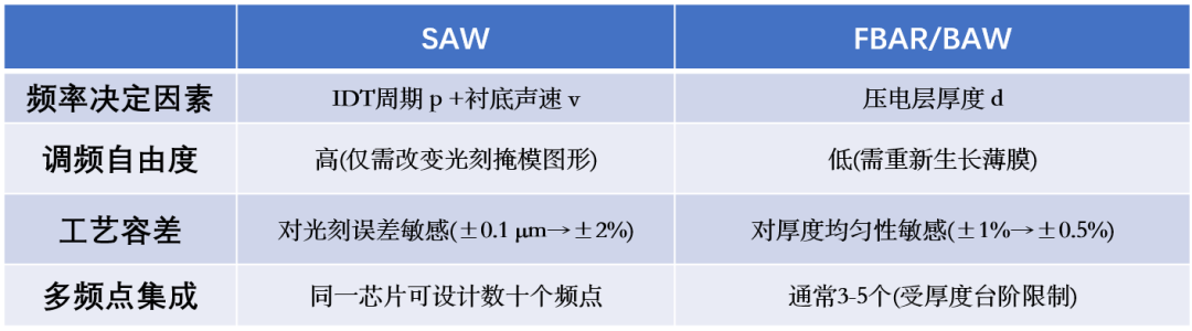
Figure 45 Comparison of the Impact of Acoustic Wave Filter Processes on Frequency
Choice is Greater than Effort
From the introduction to the SAW filter processes above, it can be appreciated that almost every step in the SAW process route can be realized through various processes and equipment. In the journey towards domestic filter production, such choices are everywhere. Faced with a dazzling array of equipment, competing process routes, and various technical solutions, every decision is crucial for the future:
-
Where is the evolution of filters headed?
-
How to choose photolithography processes?
-
Which photoresist can carry dreams?
-
Which coating technology will dominate?
-
Is the sword of conquest entrusted to the wisdom of R&D or the craftsmanship of processes?
Awakened by technological blockades, every colleague in the domestic filter field is contemplating and exploring, with diverse ideas and routes, but behind this exploration is a shared pursuit of the ultimate belief in craftsmanship.
In Conclusion
Due to space limitations and the author’s capabilities, this introduction to the SAW wafer fabrication process comes to a close. This article aims to dissect the SAW process flow from a macro perspective while analyzing the characteristics of different processes from a micro perspective, hoping to inspire beginners. Any viewpoints and content may inevitably have shortcomings, and constructive criticism is welcome.
In the first season of “A Bite of China,” it was mentioned that “Butter-fried Matsutake is more common in the Matsutake production area. Melt butter in a black pottery pot, add sliced fresh Matsutake. The oil temperature quickly removes moisture from the Matsutake surface, revealing its aroma… High-end ingredients often require the simplest cooking methods.” The secrets of the kitchen, on the surface, are the art of water and fire, but in essence, they are merely the harmonious relationship between humans and the universe. The same applies to craftsmanship.
END
About Us
ABOUT US


Scan the QR code | Follow Us
WeChat Official Account | Voice of Ruichuang
TianTong Ruichuang Technology Co., Ltd.