Why is Chip Tape-Out So Expensive?
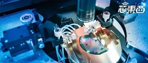
Multiple failed tape-outs may lead to the collapse of a company. The chip industry is no stranger to tape-out. The so-called tape-out refers to the process of manufacturing chips through a series of steps, akin to an assembly line. This stage is crucial as it lies between chip design and mass production. In simple terms, … Read more