
Child of the Sino-US Trade Era
On September 14, 2020, late at night, Hsinchu, Taiwan. TSMC’s factory was brightly lit, and the machines on the production line were still running at high speed, but there was an unusual tension in the air. Just a few hours earlier, the U.S. Department of Commerce announced: After September 15, any chip company using U.S. technology would not be allowed to supply Huawei without permission. At midnight on September 15, the U.S. ban officially took effect. On TSMC’s production line, all chip orders prepared for Huawei came to an abrupt halt. A historic scene unfolded as Huawei chartered a flight to bring back the last Kirin chips. This “chip rush” marked Huawei’s complete shift towards independent research and development and domestic alternatives, awakening the nation and giving wings to domestic semiconductor technology. Without this unprecedented technological sanction, it is hard to imagine that one of the 35 “bottleneck” technologies restricting our industrial development, the RF filter, would have grown wildly across the land of China in just a few years.
In the family of filters, while experienced practitioners—relatively complex cavity filters and ceramic filters—laid the foundation for communication through precision machining and high-temperature sintering processes, the new generation of SAW (Surface Acoustic Wave) filters is once again emerging with the precision “key” of semiconductor manufacturing processes. It opens a new technological route, successfully achieving a leap from macro structures to microelectronic scales, showcasing unique charm and competitiveness in the tide of miniaturization and integration.
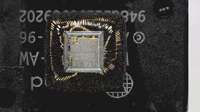
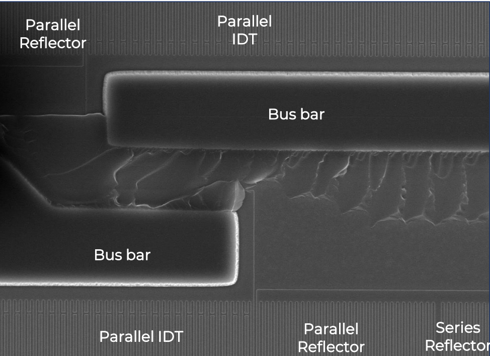
Figure 1 Comparison of SAW and high-process chip cover (Image source: Internet)
However, in the semiconductor field, SAW seems somewhat out of place. On one hand, compared to the 8-inch/12-inch fabs, SAW is relatively small, with the industry still predominantly using 4-inch/6-inch LT or LN. On the other hand, while the industry is racing towards 3nm, SAW is still developing above K-line (248nm). Furthermore, compared to the complex hundreds of photolithography steps, SAW can complete the entire wafer fabrication process with as few as three photolithography steps. In the face of the towering digital skyscrapers of chips, SAW is like a three-story small villa. Yet, this simple small villa has caused many heroes to falter. Compared to other semiconductor processes, the role of the metal layer in SAW departs from the traditional notion of conductors. More importantly, this part of the conductor (IDT) participates in the resonant action of the filter, and even slight disturbances in the IDT morphology can have a significant impact on the core performance of the filter. Figure 2 shows the core critical dimensions of SAW; the width/thickness/angle of the IDT dimensions constitute the three core elements of SAW. It is hard to imagine that a resonator composed of D=500nm and h=180nm requires the D fluctuation to be controlled within ±5nm and h within ±1nm to achieve frequency fluctuations within 1MHz, and an angle change from 75° to 85° can also cause about 0.XdB of insertion loss fluctuation. The difficulty of SAW is on a completely different dimension. When you confidently hold a Barrett rifle and can hit the target from a kilometer away, the examiner says he is more interested in the size of the bullet hole, the depth of the hole, and the angle of incidence. Figure 3 shows a simplified process diagram of the SAW filter, illustrating that photolithography, film deposition, etching, and frequency tuning constitute the basic steps of semiconductor filters. The following will mainly introduce each process step in detail.
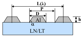
Figure 2 Core dimensions of SAW performance
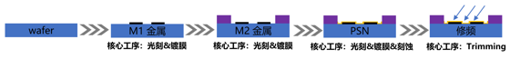
Figure 3 Simplified process diagram of SAW
Photolithography – The Crown Jewel of Semiconductor Manufacturing
From the simple process diagram of SAW, it is not difficult to see that almost every step relies on the photolithography process. Not only in SAW processes but also in other semiconductor process flows, photolithography is one of the most important links. It utilizes precision optical projection and photochemical reactions to transfer the integrated circuit design patterns from the mask onto the surface of the silicon wafer coated with photoresist with high resolution, high overlay accuracy, and high fidelity. The patterns formed serve as temporary masks, providing a precise spatial definition basis for subsequent selective etching, ion implantation, thin film deposition, or stripping processes, thereby constructing complex three-dimensional micro-nano structures on the silicon wafer. The resolution limit of photolithography directly determines the feature size and integration of semiconductor devices, making it the core engine and major technical bottleneck driving the continuation of Moore’s Law and the evolution of process nodes, rightfully earning it the title of the crown jewel of semiconductor manufacturing. When mentioning photolithography, many people immediately think of ASML, which has almost become synonymous with lithography machines. However, ASML is actually a latecomer, and it is necessary to first briefly review the history of lithography machines.
The Past and Present of Lithography Machines
In 1958, while China was still striving for industrial autonomy, the first domestically produced “Dongfeng” car and “Hongqi” luxury car were born that year. Meanwhile, in faraway Texas, on September 12, a nervous Kilby, just having left Bell Labs, connected a ten-volt power supply to the input and connected an oscilloscope to the output. At the moment of connection, a frequency of 1.2 megahertz and an amplitude of 0.2 volts appeared on the oscilloscope. The first integrated circuit made from a single material in modern electronic industry was thus born, and Kilby, the inventor of the integrated circuit, received the Nobel Prize in Physics in 2000.
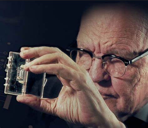
Figure 4 Kilby and the world’s first integrated circuit he invented (Image source: Internet)
When the first integrated circuit, the size of a fingernail, was born, no one probably expected that this cry would trigger a global chip revolution. However, unlike today’s engineers elegantly typing code in front of computers, the “primitive semiconductor people” of sixty years ago were performing astonishing “handmade chip” performance art. The first generation of chip engineers first drew the integrated circuit layout on paper with colored pencils. Once they completed this intricate spider web-like circuit diagram, the real magic began—holding a miniature engraving knife, they transformed the pencil lines into micron-level engravings on a poker-sized photomask. This can be considered the most hardcore “micro-sculpture art” in human history. Finally, they used a camera to reduce the master pattern by 50-100 times to obtain a photomask for lithography. The primitive lithography machine that matched this handmade photomask was the contact lithography machine. In 1961, the first contact lithography machine was manufactured by the American company GCA, which was the most advanced “lithography artifact” at that time.
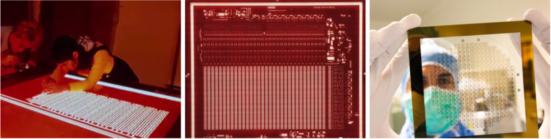
Figure 5 Engineers carving the mask and mask patterns as well as modern masks
Image source: History of lithography machine evolution (Part 1): The Beginning of Time & The Struggle for Supremacy
The Industrial Evolution of Lithography Machines – From Competition to Division of the Market
The development of lithography machines is a condensed history of the evolution of the semiconductor industry, with its technology route evolving from contact and proximity lithography to projection lithography, further branching into scanning projection, step-and-repeat, and step-and-scan. Companies from various countries have alternately led innovations during this process. The technological evolution of lithography machines began in the 1960s, initially using contact lithography technology (where the mask directly contacts the photoresist). The first device was launched by the American company GCA in 1961, but it was replaced by proximity lithography due to contamination and mask wear issues. The latter reduced damage by leaving a gap between the mask and the wafer, but diffraction effects limited the resolution (about 2μm). In the 1970s, projection lithography emerged, with PerkinElmer introducing scanning projection lithography machines that improved imaging quality using optical lenses. In 1978, GCA launched the stepper lithography machine, achieving 1μm resolution through step-and-repeat exposure, becoming mainstream. In the 1980s, Japan’s Nikon entered the competition with the NSR-1010G, sharing the market with GCA. After ASML was established in 1984 from Philips Labs, it promoted the upgrade of step technology to step-and-scan, combining dynamic scanning with reduced projection lenses (5:1), enhancing precision and efficiency. After 2000, technological competition focused on shortening the wavelength of light sources. Nikon dominated 157nm dry lithography, but ASML took a different path, launching immersion lithography in 2003 in collaboration with TSMC, injecting high-refractive-index liquids (water) between the lens and the wafer, effectively reducing the 193nm light source to an equivalent wavelength of 134nm, breaking through the resolution bottleneck and surpassing Nikon. Since then, ASML has monopolized the high-end market, launching extreme ultraviolet lithography (EUV) in 2013, using a wavelength of 13.5nm, pushing the process into nodes below 5nm.
In terms of vendor landscape, early leaders included the American GCA and PerkinElmer, but in the 1980s, Nikon overtook them. GCA went bankrupt in 1993 due to technological lag, leading to Japan monopolizing 80% of the global market. ASML acquired key technologies through the acquisition of SVG and rose through immersion innovation, reaching a 60% market share by 2007, ultimately achieving global monopoly with EUV. The rise and fall of vendors confirm that the choice of technological route is decisive. The U.S. pioneered the concept, Japan optimized mass production, while ASML achieved a comeback through open cooperation (with TSMC and Zeiss) and disruptive innovation (immersion). Did you know? The manufacturing of EUV lithography mirrors is considered an engineering miracle: it requires the precise deposition of 40 alternating layers of silicon/molybdenum on a substrate, with each layer’s thickness deviation not exceeding a single atomic dimension. The overall flatness requirement is so stringent that it is akin to maintaining the height difference across all of China within a range of 1 millimeter—this is a concrete manifestation of the core precision of lithography machines.
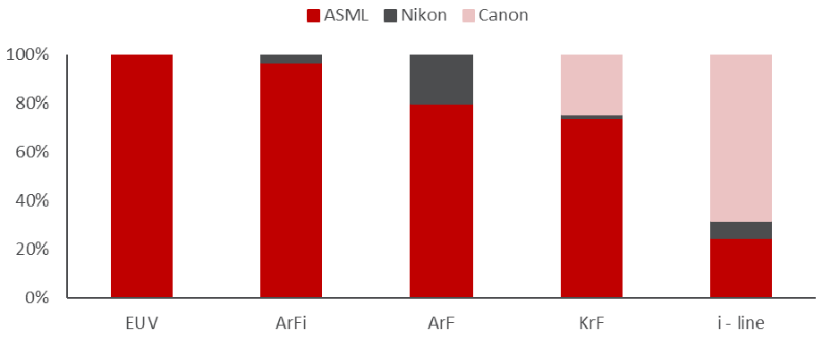
Figure 6 Global lithography machine market share (Image source: Internet)
Considering the trend of miniaturization in electronic devices, reducing the feature size of individual transistors is the primary method for the development of integrated circuits. The reduction in transistor size can lower power consumption, increase the response speed of integrated circuits, and increase the number of transistors per unit area on the chip. The minimum feature size is also known as the Critical Dimension (CD). The minimum resolution achievable by lithography machines is determined by the Rayleigh criterion, which states that CD=k1*λ/NA, primarily involving three core indicators: wavelength (λ), numerical aperture (NA), and process factor (k1). Among these, the reduction of the light source wavelength λ is the most important technological evolution direction for lithography machines. The global lithography machine light source has undergone several evolutions from 436nm-365nm-248nm-193nm-13.5nm (Figure 7). Taking the evolution of the light source from ArF (193nm) to EUV (13.5nm) as an example, if other factors remain the same, its resolution can be directly improved to about 0.07, making it one of the most effective paths. Mainstream lithography machines have experienced several generations of wavelength evolution, and the corresponding light sources have also undergone iterations from UV light sources (G-line, I-line), DUV light sources (KrF, ArF/ArFi), to EUV light sources, with different product forms and working principles.
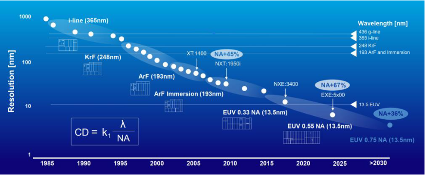
Figure 7 Lithography machine resolution improvement nodes (Image source: ASML official website)
From a technological evolution perspective, lithography machines have transitioned from contact and proximity to projection lithography, with each generation of technology iteration significantly improving lithography resolution and efficiency. Specifically, the earlier technology routes were contact and proximity lithography machines, both of which had limited resolution. Later technology routes were projection lithography machines, including step-and-repeat and step-and-scan, with the latter being more suitable for high-density integration, improving exposure uniformity and field size through dynamic scanning, adapting to smaller process nodes.
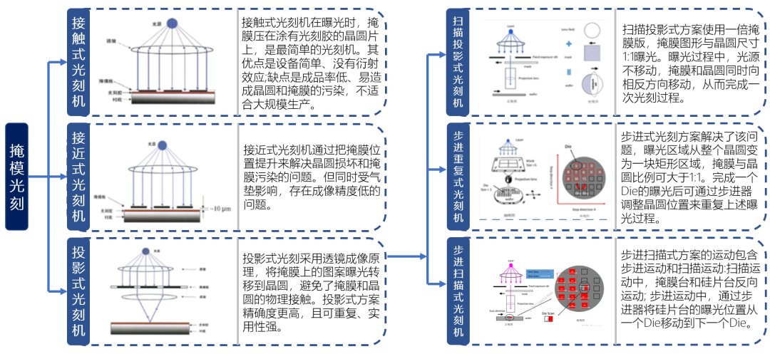
Figure 8 Main classifications of lithography machines (Image source: Internet)
The Entrepreneurial History of Domestic Lithography Machines
Nikon and Canon from Japan began entering the lithography machine field in the late 1960s. China’s start was not late either, roughly beginning around the same period to use lithography technology to manufacture integrated circuits. In 1965, China’s first integrated circuits were successively produced in Beijing, Shijiazhuang, and Shanghai. In September 1974, the first national large-scale integrated circuit industrial conference was held, focusing on the research and development of large-scale integrated circuits and materials, equipment, breakthroughs in ultra-micro particle dry plates, photoresists, ultra-pure reagents, high-purity gases, and electron beam deposition machines with magnetic field deflection. The development history of domestic lithography machines reflects a difficult breakthrough from early independent exploration to technological blockade. In the 1960s to 1980s, the gap between China and the international community was relatively small, but due to economic constraints and the mindset of “buying rather than making,” it gradually fell behind. After 2000, under the push of national strategy, companies like Shanghai Microelectronics restarted R&D, gradually achieving mass production at 90nm. In recent years, domestic lithography machines have achieved a global leading position in the packaging field and have made breakthroughs in the localization of core components of DUV lithography machines. However, compared to international top levels, there is still a generational gap in advanced processes. In the future, through innovative technological paths such as solid-state light sources, China is expected to achieve a “shortcut” in the lithography machine field, but challenges such as mass production stability and industrial chain support need to be addressed.
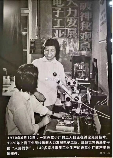
Figure 9 Chinese lithography engineers discussing lithography technology (Image source: Internet)
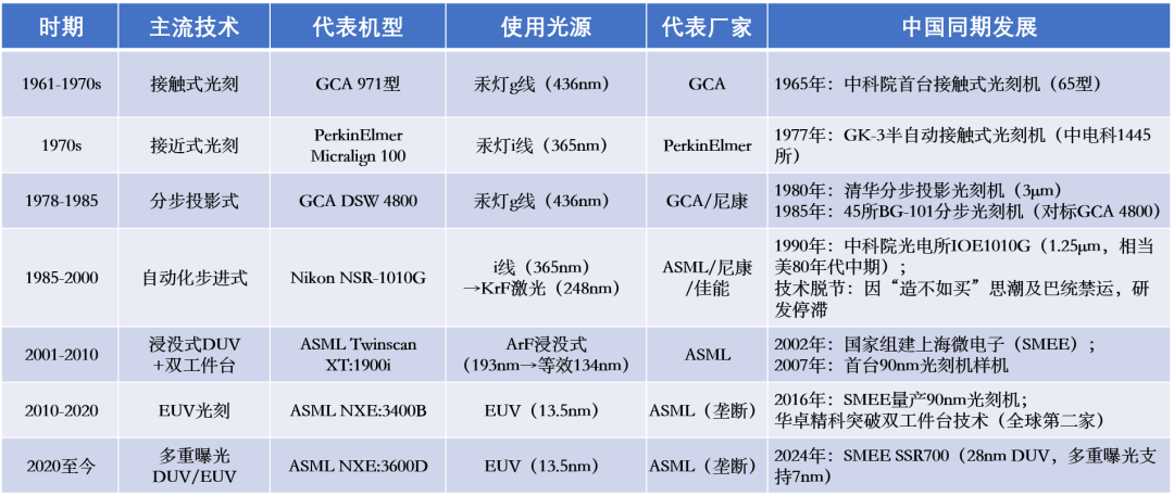
Figure 10 The development history of lithography machines
Photolithography Partner: The Art of Balancing Resolution
Photoresist can be considered the “veteran partner” of lithography machines, with a history far older than that of lithography machines. As early as 1822, French inventor Joseph Nicéphore Niépce was experimenting with a kind of “sunlight development” black technology. His experimental tools were only simple oil paper, glass plates, and asphalt that could dissolve in vegetable oil. Niépce wanted to replicate the patterns on the oil paper and came up with a brilliant idea: he covered the glass with oil paper coated with “asphalt paste” and then exposed it to sunlight. A miraculous thing happened: the areas exposed to sunlight became indestructible, while the parts in the shadow could be cleaned with rosin and vegetable oil, revealing the pattern! In this experiment, asphalt can be considered the original version of photoresist. Who would have thought that the asphalt on the road today would become the ancestor of future precision chip manufacturing? However, it wasn’t until more than a century later that it truly took the stage, making a significant impact on printed circuit boards, ultimately becoming an indispensable cornerstone of modern semiconductor processes—from asphalt drawings on oil paper to nano-level circuit engravings, the technological leap is astonishing. In 1925, American Kodak discovered that polyvinyl alcohol and cinnamic acid ester had a strong crosslinking reaction under ultraviolet light and high photosensitivity, which was later used for optical glass grating etching, becoming a pioneer of photoresist. In 1954, Kodak developed the first photoresist with polyvinyl alcohol and cinnamic acid ester with light-curing properties, branded as KPR.

Figure 11 The ancestor of photoresist, Niépce (Image source: Internet)
The development of lithography machines and photoresists has always shown a close synergistic relationship, with both forming the core technological pillar of semiconductor manufacturing. Lithography machines, as precision devices for “sculpting” chip patterns, directly drive the performance innovation of photoresists. For example, lithography machines have evolved from early UV full-spectrum to deep UV and even extreme UV, with each reduction in exposure wavelength requiring photoresists to possess higher resolution, lower line width roughness, and stronger etch resistance. Taking EUV lithography machines as an example, their extremely short wavelength of 13.5nm requires photoresists to have higher photon absorption efficiency and chemical sensitivity, while traditional photoresists cannot meet this demand, leading to the development of new types of EUV photoresists such as metal oxides.
Photoresists can be mainly divided into positive and negative resists, with the core difference between positive and negative resists being the photochemical reaction and development results in the exposed areas. Negative resists undergo crosslinking and curing under UV light, containing photosensitive polymers and crosslinking agents. During exposure, the crosslinking agent decomposes to produce active free radicals, initiating polymer crosslinking, resulting in a significant increase in molecular weight and decreased solubility in the exposed area. During development, the unexposed parts are dissolved by the solvent, while the exposed area is retained due to crosslinking. However, crosslinking can easily lead to swelling during development, limiting resolution. Positive resists achieve patterning through photodecomposition, containing photoacid generators and base-soluble resins. During exposure, the photoacid generator decomposes to produce strong acid, which catalyzes the deprotection reaction of the resin during the post-bake stage, converting the hydrophobic resin into hydrophilic carboxylic acid groups. During development, the exposed area dissolves rapidly due to carboxyl ionization, while the unexposed area remains insoluble. This mechanism avoids swelling issues, allowing for resolution down to the nanometer level.
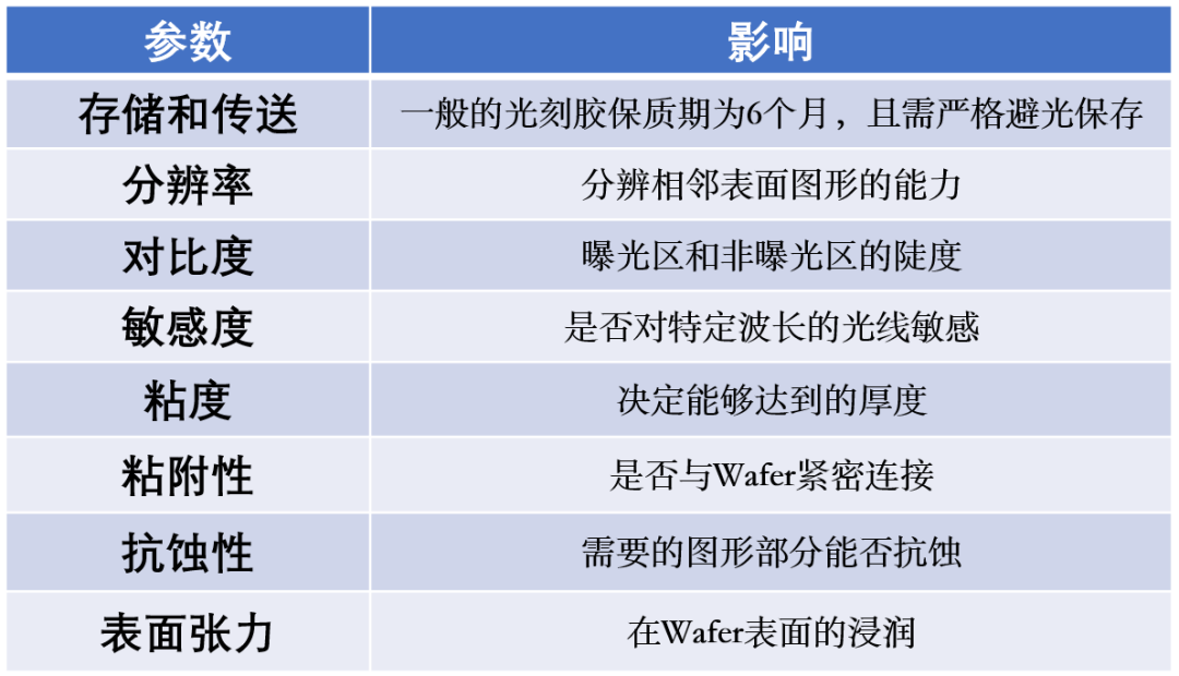
Figure 12 Differences between positive and negative photoresists
The core performance requirements of photoresists are to achieve a precise balance between extreme resolution, sensitivity, line width roughness, etch resistance, and process window. While resolution is a key indicator, it is not the only core factor. The principle is that resolution is determined by the optical diffraction limit and the chemical contrast of the photoresist. For example, chemically amplified resists (CAR) catalyze the deprotection reaction through photoacid generators, forming a high dissolution rate difference between the exposed and unexposed areas, allowing for nanometer-level patterns. However, if one purely pursues resolution, it may require reducing the concentration of the photosensitizer or enhancing acid diffusion suppression, which would lead to a deterioration in sensitivity and increase line width roughness. Additionally, insufficient etch resistance can lead to pattern distortion during plasma etching, degrading critical dimension control, while a narrow process window means that micro-vibrations in the equipment can directly lead to wafer scrapping. Therefore, advanced photoresists resolve contradictions through material innovations: CAR utilizes catalytic cascade reactions to simultaneously optimize resolution and sensitivity; monodisperse molecular glass structures suppress line width roughness (LWR); and multilayer resist architectures balance pattern transfer accuracy and etch selectivity. Any single performance shortcoming can lead to chip failure, so the true core of photoresists lies in the system balance under multi-parameter limits.
Figure 13 Core performance parameters of photoresists
The core difficulty of domestic photoresist localization lies in the synthesis and purification processes of high-end resins, which directly restrict the autonomy and controllability of high-end photoresists such as ArF and EUV. Resins account for 50% of the cost of photoresists, and the precision of their molecular structure directly determines exposure accuracy and etch resistance. Domestically, only 8%-10% of high-end categories can be covered in the monomer purification stage, while resin purification requires additional separation of metal impurities, which is more complex, and domestic equipment compatibility is insufficient, leading to excessive metal residues and poor batch stability. 80% of photoresist solvents are monopolized by foreign companies such as Dow Chemical and BASF, and domestic solvents lack sufficient purity, easily causing wafer contamination. Even the specialized containers for photoresists need to be imported, and due to low domestic demand, it is difficult to support production line construction. At the same time, Japanese companies hold 90% of EUV photoresist patents and lead technology standards through the IMEC alliance, blocking domestic replacement paths. Localization needs to prioritize overcoming the monomer purification → resin synthesis → integrated formulation chain. Currently, if the resin purification bottleneck is broken, the localization rate of KrF/ArF (currently 1%-5%) is expected to rise to over 30%, but EUV still requires long-term technological accumulation.
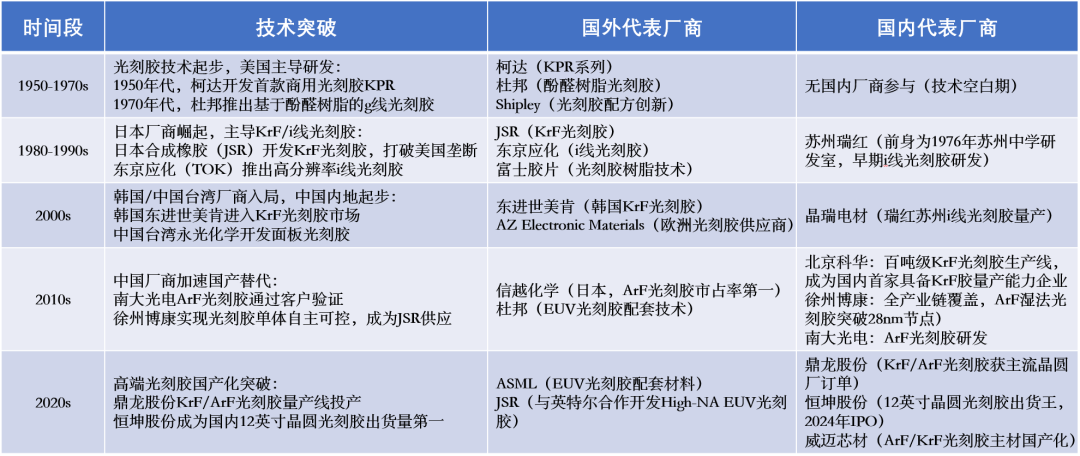
Figure 14 Development history of photoresists
Track: The Perfect Combination of Coating, Exposure, and Development
If we compare lithography machines to a stove that can precisely control the heat, then photoresist is the oil used for cooking, and the coating and developing machine is that magical smart pot—automatically controlling temperature and rotating without burning the bottom. Coating and developing equipment is often referred to as Track, and the most fitting explanation is that it plays the role of an “automated transport and processing track” for wafers in the lithography process. It defines the route and processing sequence that the wafer must follow from entering the equipment to completing all photoresist-related processing steps (coating, thermal treatment, development) and seamlessly collaborates with the lithography machine to complete the entire lithography process. A single coating, exposure, and development constitutes the basic unit of lithography, differing only in the selection of different masks and the use of different photoresists to achieve different lithography effects.
In the 1980s, the top 10 semiconductor equipment manufacturers were dominated by American companies, occupying 90% of the market. At that time, many Japanese trading companies represented these American semiconductor equipment companies’ devices. Later, Japanese semiconductor equipment entered a period of rapid development. By the 1990s, the rankings of semiconductor equipment manufacturers changed dramatically, with giants being Japanese companies, among which Tokyo Electron (TEL, Japan) quickly occupied the market with Track equipment, becoming the leader. As of now, TEL has become the global monopolist of Track equipment, with a market share of 90%, far exceeding the second place, Japan’s DNS (5%), covering all lithography nodes from I-line to EUV, meeting various process needs. Especially in advanced processes below 28nm, it almost monopolizes the market with ArFi immersion equipment. Fortunately, coating and developing equipment has transitioned from complete reliance on imports to domestic mass production of 28nm equipment, with a few manufacturers like ChipSource Micro and Shengmei achieving a “0 to 1” breakthrough in ten years. However, the current localization rate is less than 5%, and international giants still dominate advanced processes (especially EUV). Domestic manufacturers need to accelerate breakthroughs in process stability, lithography machine collaboration, and nodes below 14nm. TEL collaborates with lithography machine giants like ASML and Nikon to develop interface protocols, ensuring seamless connectivity with lithography machines, forming a closed ecosystem of “lithography machine-Track” (In-Line), providing TEL with significant user stickiness. Offline refers to the separation of lithography machines, coating machines, and developing machines, with no direct physical connection integrated together. For example, after completing the coating process, the operator needs to manually take the coated wafer and place it into the exposure machine for exposure, and after exposure, it must be manually placed into the developing machine for development. In contrast, In-line allows the lithography machine/coating/developing machines to form a continuous whole. After the operator places the material in the first step, no further operations are required on the wafer during the coating-exposure-development process, which is automatically completed.
Figure 15 Evolution diagram of TEL’s Track (Image source: Internet)
The close cooperation between lithography machines and Track, with coating, exposure, and development forming a broadly defined basic unit of lithography, is illustrated in Figure 16.
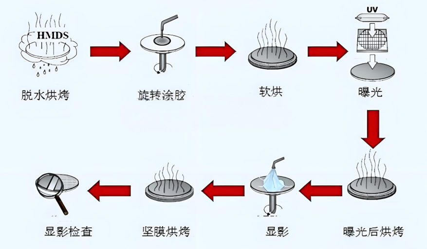
Figure 16 Coating, exposure, and development process diagram (Image source: Internet)
1. HMDS (Hexamethyldisilazane):After cleaning, the wafer undergoes high-temperature baking, and then HMDS is vaporized and coated onto the wafer surface, changing the wafer surface from hydrophilic to hydrophobic, altering the adhesion of the photoresist to the wafer surface.
2. Coat (Coating):Photoresist is evenly coated on the wafer surface to achieve the desired film thickness, ensuring uniformity and defect-free surface of the photoresist on the wafer. The coating process steps are: a) The wafer is transferred to a flat, rotatable chuck and vacuum-suctioned from the back, rotating together with the chuck; b) The photoresist solution is sprayed onto the wafer; c) The rotating chuck accelerates until the desired film-forming speed is reached; d) After reaching the desired speed, it continues for a certain time to ensure the photoresist is more uniform on the wafer surface. The centrifugal coating of the coating machine is akin to the rotation of a pancake griddle: the former flings out a nanometer-level film at 30000rpm/s acceleration, while the latter uses wrist strength to flip out millimeter-level batter.
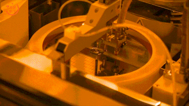
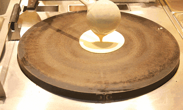
Figure 17 Coating and pancake flipping (Image source: Internet)
3. Soft Bake:The liquid photoresist contains 65%-85% solvent. After coating, there is still 10%-30% solvent remaining, which needs to be baked at a certain temperature to evaporate the excess solvent from the photoresist. This step is called soft bake.
4. Exposure:The light emitted from the illumination source is focused through a lens onto the mask, generating diffracted light beams that carry the pattern information from the mask. The light beams are focused onto the wafer surface through the projection lens, forming the mask pattern on the wafer surface. As mentioned earlier, photoresists are mainly divided into positive and negative resists. The parts of positive resists exposed to the light source will decompose and be washed away by the developer, while the parts of negative resists exposed to the light source will undergo crosslinking reactions and be retained after development.
The Magical Positive Trapezoid:Due to scattering and diffraction of light within the resist layer, when the developer dissolves from top to bottom, the top exposed area dissolves more thoroughly, forming a positive trapezoid. The exposed area of negative resists undergoes crosslinking and curing, and during development, the unexposed parts are dissolved. Since the light intensity near the substrate is weaker, the degree of crosslinking is lower, leading to slightly more dissolution at the bottom, resulting in a cured structure that presents an inverted trapezoid. This morphological difference directly affects the precision of subsequent etching or deposition processes, resulting from the combined effects of the chemical properties of the photoresist and optical effects.
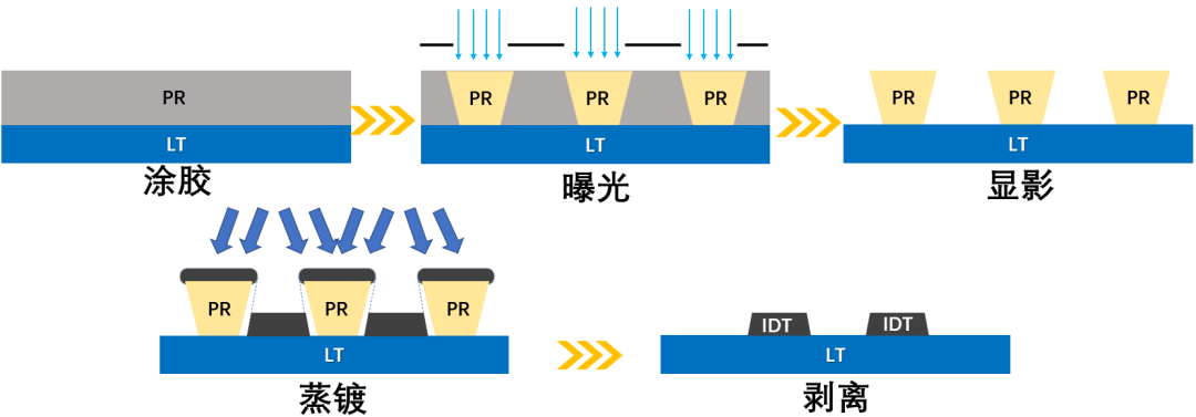
Figure 18 Morphological differences between positive (left: positive trapezoid) and negative (right: inverted trapezoid) resists (Image source: Internet)
It is precisely because of the use of negative resists in the Liftoff process that the IDT of most SAW filters appears as a positive trapezoid in actual FIB cross-sectional images.
Figure 19 Schematic diagram of the Liftoff process forming a positive trapezoid IDT
5. Post-Exposure Bake:Post-exposure bake refers to the baking process of the photoresist after exposure, generally conducted on a hot plate at 110℃-130℃. Its purpose is to enhance the adhesion of the photoresist and reduce standing wave effects.
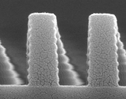
Figure 20 Morphology of photoresist after PEB (Image source: Internet)
6. Development:Development is the process of removing or retaining the exposed photoresist on the wafer. After the development time is reached, the wafer surface is immediately rinsed with deionized water, which not only stops the development but also washes away any residual photoresist generated during development. During this process, the wafer must be spun at a specified speed to generate centrifugal force, achieving the desired pattern. The developing tank is like a miniature reactor, with the developing solution at 38℃ precisely reacting with the photoresist under ±0.1℃ temperature control. Engineers use semiconductor-grade PID algorithms to control the heating rods, while darkroom technicians rely on their intuition to judge the “breathing rhythm” of the water bath—both are combating temperature disturbances of about 1℃ in the plastic developing tank.
Figure 21 Development and darkroom photo washing art (Image source: Internet)
The Mystery of the Yellow Light Zone – The UV Sensitivity of Photoresists
Are you curious why every fab’s photolithography workshop uses yellow light bulbs while the deposition workshop uses white light? The first time I entered the yellow light zone, I was equally puzzled. This is because photoresists are extremely sensitive to ultraviolet light (UV), especially in the deep UV/DUV and extreme UV/EUV bands. If the ambient light contains ultraviolet components (such as sunlight or ordinary white light), it can inadvertently expose the coated wafer, leading to pattern distortion or even scrapping. The yellow light environment (usually using sodium lamps, wavelength ≈589nm) is a carefully selected safe light source that avoids the UV band; yellow light does not contain ultraviolet components and will not trigger chemical reactions in photoresists. At the same time, yellow light provides sufficient illumination for operators/engineers to operate equipment and visually inspect. So why not use red or green light? Red light (with a longer wavelength) is safer but has poor illumination and can easily cause drowsiness. Green light may contain short-wavelength components close to blue/UV (higher risk), and early sodium lamp technology was mature and cost-effective.
Thus, a brief introduction to the most important step in the SAW wafer fabrication process, photolithography, has been provided. The subsequent sections will detail the corresponding processes of thin films, etching, and more.To be continued…
About Us
ABOUT US


Scan the QR code | Follow us
WeChat Official Account |Voice of Ruichuang
TianTong Ruichuang Technology Co., Ltd.