
Follow our public account, click the top right corner of the public account homepage ” · · · “, set a star mark, and stay updated on the latest news in automotive semiconductors.
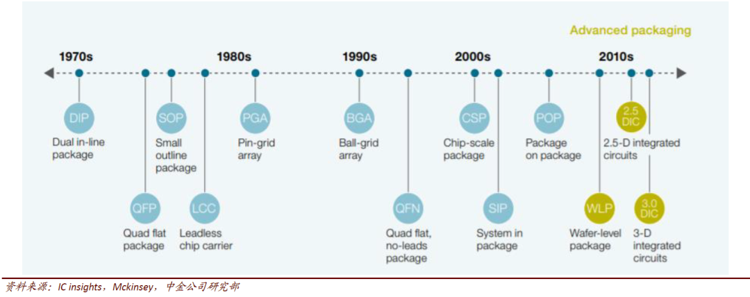
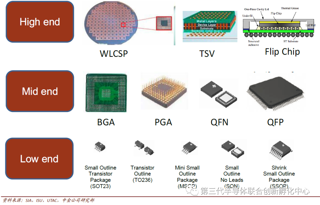
There are many packaging forms for semiconductor devices, which can be classified into three categories based on their shape, size, and structure: pin-insertion type, surface mount type, and advanced packaging. From DIP, SOP, QFP, PGA, BGA to CSP and SIP, the technical specifications have advanced with each generation.
Overall, semiconductor packaging has undergone three major innovations:The first was in the 1980s, transitioning from pin-inserted packaging to surface mount packaging, which greatly increased the assembly density on printed circuit boards; the second was the emergence of ball grid array packaging in the 1990s, which met the market’s demand for high pin counts and improved the performance of semiconductor devices; chip-scale packaging and system packaging are products of the current third innovation, aimed at minimizing the packaging area.
1
Basic Concepts of Semiconductor Packaging and Testing
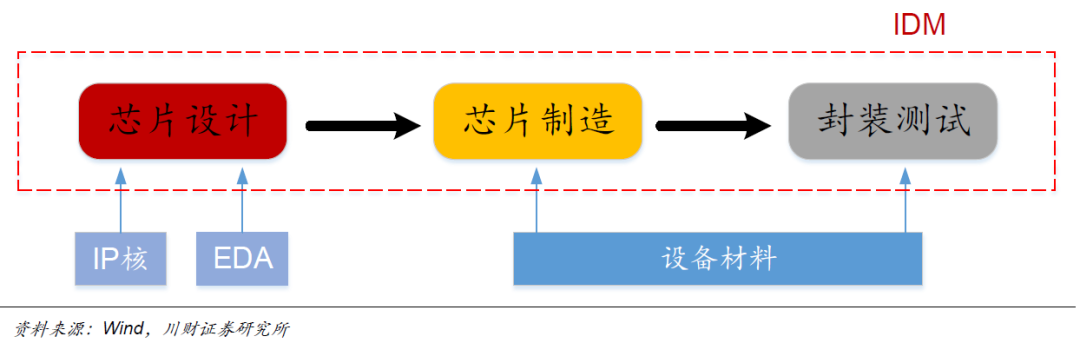
The semiconductor industry chain includes chip design, chip manufacturing, packaging, and testing, with downstream covering various industries. Additionally, service support for the industry chain includes companies providing IP cores and EDA design tools for chip design, as well as companies providing equipment and material support for the manufacturing and packaging testing stages.
▼ Overview of the Semiconductor Industry Chain
Integrated circuit packaging and testing include two stages: packaging and testing. Packaging protects the chip from physical, chemical, and environmental damage, enhances the chip’s heat dissipation performance, achieves electrical connections, and ensures the circuit operates normally; testing primarily involves functional and performance testing of chip products, filtering out products that do not meet functional and performance requirements.
Currently, packaging technology is gradually evolving from traditional lead frames and wire bonding to advanced packaging technologies such as flip chip (FC), through-silicon via (TSV), embedded packaging (ED), fan-in/fan-out wafer-level packaging, and system-in-package (SiP). Chip sizes continue to shrink, pin counts increase, and integration levels continue to rise.
Different packaging types have different process flows, and relevant testing is required during and after packaging to ensure product quality.
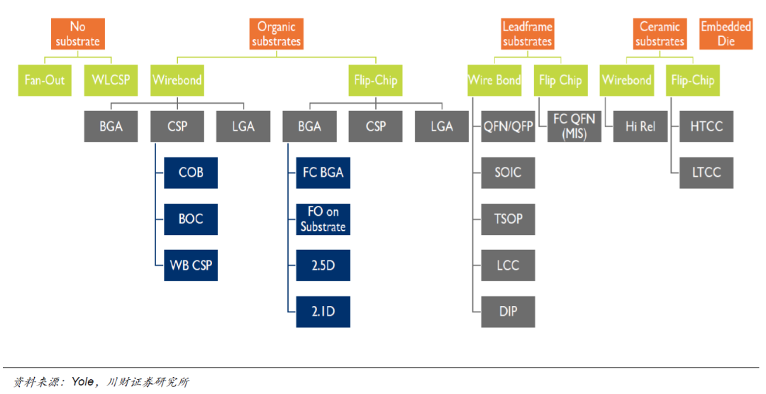
▼ Advanced Packaging Series Platforms for Semiconductors
2
Trends in the Semiconductor Packaging and Testing Industry
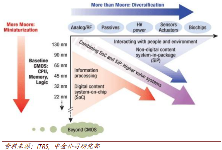
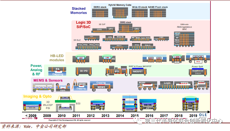
Semiconductor products are evolving from two-dimensional to three-dimensional. In terms of technological development, new packaging methods such as system-in-package (SiP) have emerged, and in terms of implementation methods, advanced packaging technologies such as flip chip, bumping, wafer-level packaging, 2.5D packaging, and 3D packaging (TSV) have appeared.
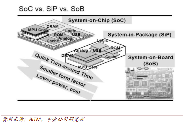
SoC vs. SiP ► SoC:Short for System-on-Chip, SoC is a highly integrated chip product containing different functional circuits within a single chip.
► SiP:Short for System-in-Package, SiP integrates multiple functional chips, including processors and memory, within a single package to achieve a complete basic function. As Moore’s Law slows down, the semiconductor industry is gradually entering the post-Moore era, where both SoC and SiP are ways to achieve higher performance at lower costs.
Generally, in terms of integration, SoC has higher integration, lower power consumption, and better performance; while SiP has advantages in flexibility, broader compatibility, lower costs, and shorter production cycles. Therefore, for products with relatively long life cycles, SoC is more suitable.
For products with short life cycles and small areas, SiP has more advantages and higher flexibility.
▼ Moore’s Law vs. Beyond Moore
▼ SiP vs. SoC vs. SoB
Traditional Packaging vs. Advanced Packaging
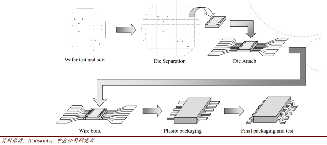
The concept of traditional packaging began after the initial through-hole transistor era. The traditional packaging process is as follows: after cutting the wafer into dies, the dies are attached to the corresponding lead frame pads, and then wires are used to connect the chip’s bonding pads to the lead frame pins (Wire Bond), achieving electrical connections, and finally, the package is protected (Mold or Encapsulation). Typical packaging methods include DIP, SOP, TSOP, QFP, etc.
3
Development Process of the Packaging Industry
Advanced packaging mainly refers to flip chip, bumping, wafer-level packaging, 2.5D packaging, and 3D packaging technologies.
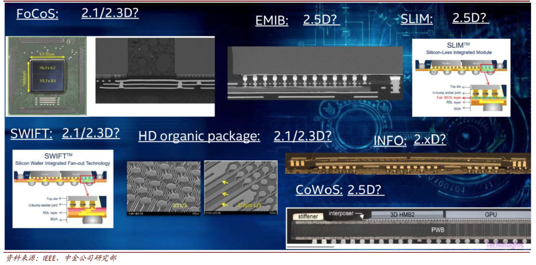
At its inception, advanced packaging only had a few options like WLP, 2.5D packaging, and 3D packaging. In recent years, the development of advanced packaging has exploded in various directions, with each company developing related technologies independently naming and trademarking their technologies, such as TSMC’s InFO, CoWoS, ASE’s FoCoS, and Amkor’s SLIM, SWIFT, etc.
Although many advanced packaging technologies have only minor differences, a large number of new names and trademarks have been registered, leading to a plethora of different types of advanced packaging in the industry, often driven by customized product demands.
IEEE introduced a 2.x naming convention at the Electronics Components and Technology Conference in May 2018, but the industry’s acceptance of this naming method remains to be seen. We will mainly discuss technologies such as flip chip, bumping, wafer-level packaging, 2.5D packaging, and 3D packaging in the field of advanced packaging.
▼ IEEE Advanced Packaging Naming Convention
Traditional Packaging Testing Process:
►Packaging:Integrated circuit packaging is the final step in semiconductor device manufacturing.
Packaging refers to the process of placing the manufactured semiconductor device into a plastic, ceramic, or metal shell that provides support and protection, and connects it to external driving circuits and other electronic components.
Packaged semiconductor devices can operate in higher temperature environments and resist physical damage and chemical corrosion. Packaging provides better performance and durability for semiconductor devices.
►Testing:Testing here refers to post-packaging testing of semiconductors.
Testing confirms the structure and electrical functionality of the manufactured semiconductor components, aiming to eliminate chips with poor electronic functionality to ensure that their performance meets system requirements.
Testing can also be referred to as “final testing,” which differs from wafer probe testing (pre-packaging testing).
▼ Simplified Traditional Packaging Process
Advantages of Advanced Packaging:
Advanced packaging improves processing efficiency, enhances design efficiency, and reduces design costs.
Advanced packaging mainly includes flip chip (Bumping), wafer-level packaging (WLCSP, FOWLP, PLP), 2.5D packaging (Interposer), and 3D packaging (TSV).
Taking wafer-level packaging as an example, products are produced in batches in wafer form, utilizing existing wafer preparation equipment, and packaging design can be conducted simultaneously with chip design. This will shorten design and production cycles and reduce costs.
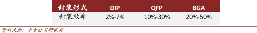
Advanced packaging improves packaging efficiency and reduces product costs. With the arrival of the post-Moore’s Law era, traditional packaging can no longer meet demands. The packaging efficiency of traditional packaging (bare chip area/substrate area) is low, leaving significant room for improvement.
In cases where chip processing is limited, improving packaging is another avenue. For example, the maximum packaging efficiency of QFP is 30%, meaning that 70% of the area will be wasted. DIP and BGA waste even more area.
▼ Efficiency of Traditional Packaging Technologies
▼ Classification of Semiconductor Packaging Products
Advanced packaging is driven by higher efficiency, lower costs, and better performance. Advanced packaging technology emerged in the 1990s, achieving electrical interconnection through point-to-line methods, resulting in higher density integration and significantly reducing area waste.
SiP technology and PoP technology laid the foundation for the advanced packaging era, while 2D integration technologies such as Wafer-Level Packaging (WLP), Flip-Chip, and 3D packaging technologies like Through-Silicon Via (TSV) further reduce the connection distance between chips, improving component response speed, and will continue to advance the field of advanced packaging in the future.
4
Advanced Packaging Technologies and Development Trends
Advanced Packaging:Flip-Chip & Bumping FlipChip refers to the flip chip technology, where previous packaging technologies placed the active area of the chip facing up, away from the substrate and attached by wire bonding.
In contrast, FlipChip places the active area of the chip facing the substrate, achieving interconnection through solder bumps (Bumping) arranged in an array on the chip.
The silicon wafer is directly mounted onto the PCB in a flipped manner, with I/O connections extending outward, significantly shortening interconnection lengths, reducing RC (Resistance-Capacitance) delays, and effectively improving electrical performance.
Advantages of FlipChip include:
Small size, enhanced functionality (increased I/O count), improved performance (shorter interconnections), increased reliability (flip chip can reduce interconnection pin counts by 2/3), and enhanced heat dissipation (the back of the chip can effectively cool).
▼ Flip-Chip Process Flowchart
Bumping is a new method of electrical interconnection between the chip and substrate. It can be achieved through small spherical conductive materials known as bumps, and the process of creating these conductive spheres is called bumping.
When the die with bumps is flipped (Flip-Chip) and aligned with the substrate, the die easily connects with the substrate pads.
Compared to traditional wire connections, Flip-Chip offers numerous advantages, such as smaller package sizes and faster device speeds.
▼ Bumping Illustration
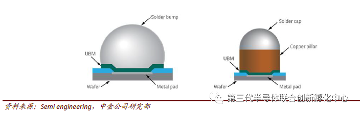
A key step in FlipChip is Bumping, which can be achieved by depositing epitaxial materials on the wafer.
Once the chip manufacturing process is complete, the Underbump Metallization (UBM) pads will be used to connect the chip to the circuit, and bumps will be deposited on the pads.
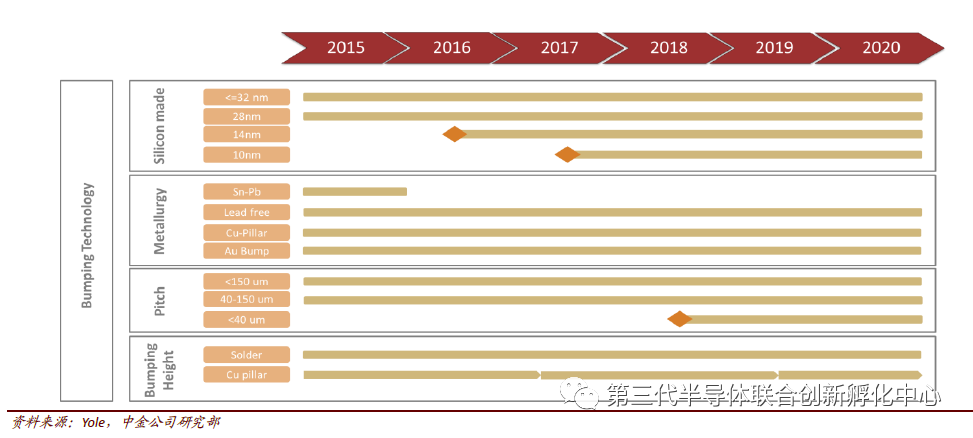
Solder balls are the most common bumping material, but gold, silver, copper, and cobalt are also good choices depending on different requirements. For high-density interconnections and fine pitch applications, copper pillars are a new material.
Solder balls deform during connection, while copper pillars maintain their original shape, which is why copper pillars can be used for denser packaging.
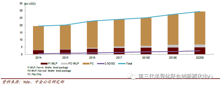
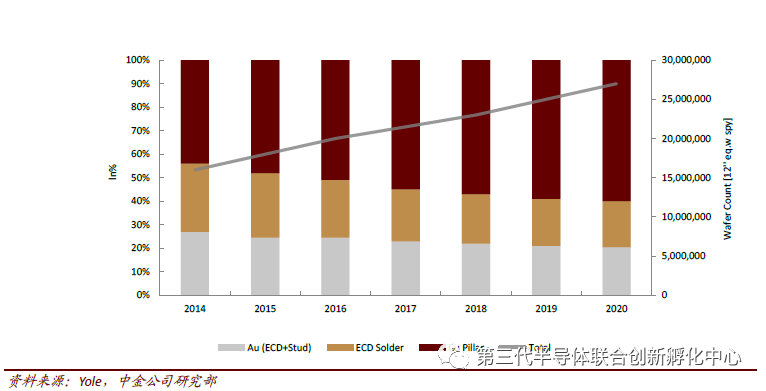
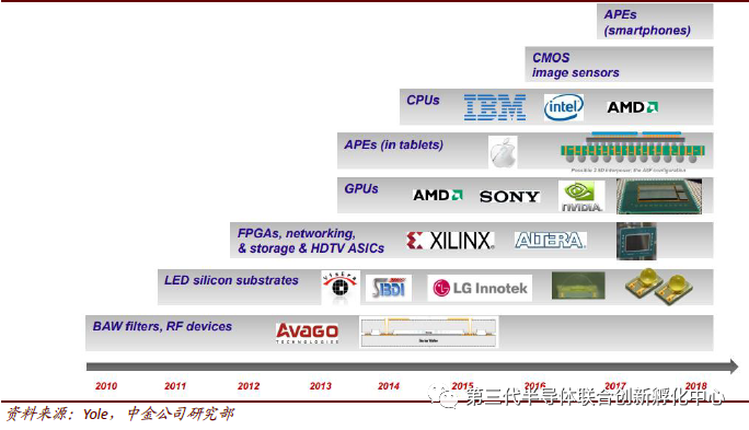
FlipChip is a major driving force for the growth of advanced packaging. According to Yole, driven by mobile wireless (especially smartphones), LEDs, and CMOS image sensors, the demand for flip chips is expected to grow from 16 million units (equivalent to 12-inch wafers) in 2014 to 32 million units by 2020, with a market value reaching $25 billion.
▼ Advanced Packaging Market Development Forecast
▼ Bumping Technology Development Path
Growth rates for FlipChip products corresponding to different bumping types vary. According to Yole, the shipment volume of integrated circuits using flip chip technology is expected to grow steadily, with capacity expanding at a compound annual growth rate of 9.8%, from approximately 16 million 12-inch wafers in 2014 to 28 million by 2020.
End applications mainly include computing chips, such as CPUs, GPUs, and chipsets for desktop and laptop computers.
Among them, gold-plated wafer bumps are expected to grow steadily, driven by the market for IC display drivers (4K2K ultra-high-definition TVs and high-definition, large-screen tablets and smartphones).
Capacity is expected to expand at a compound annual growth rate of 4%, from 4.3 million units in 2014 to 5.4 million units by 2020.
Gold stud bumps are expected to see a slight decline in capacity, from 304,000 units in 2014 to 293,000 units by 2020, mainly due to RF devices shifting from flip chip to wafer-level chip size packaging (WLCSP).
However, demand for emerging applications will increase, such as CMOS image sensor modules and high-brightness LEDs. The demand for middle-end process technologies will lead to cross-industry competition.
The emergence of middle-end process infrastructure for 3DIC and 2.5D interposer platforms will benefit fabs and IDMs, with OSAT benefiting to a lesser extent.
The development of 2.5D interposer platforms will shift value from substrate suppliers to front-end foundries.
▼ Flip Chip Development Trends by Bumping Type
Advanced Packaging:FIWLP & FOWLP, PLP First, we need to mention the concept of Wafer-Level Packaging (WLP). In traditional packaging concepts, wafers are first cut into small dies, and then connections and encapsulation are performed.
In contrast, wafer-level packaging completes the packaging of dies before cutting, with protective layers attached to the front or back of the wafer, and electrical connections made before cutting.
▼ Wafer-Level Packaging Illustration
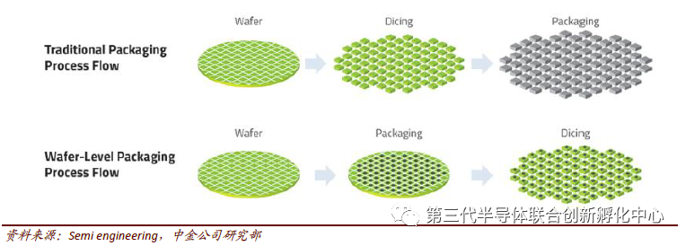
▼ Wafer-Level Packaging Process Flowchart
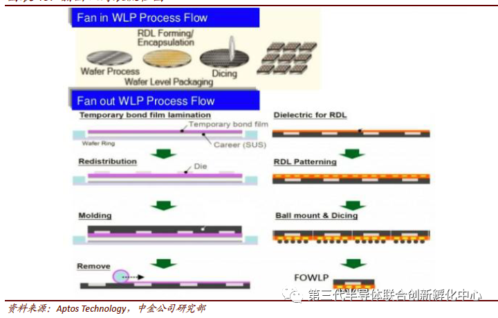
FIWLP:Short for Fan-in Wafer-Level Packaging, also known as WLCSP (Wafer-Level Chip Scale Package), fan-in wafer-level packaging is the traditional wafer-level packaging where the cutting of dies occurs last, suitable for integrated circuits with low pin counts.
As the number of signal output pins for integrated circuits increases, the size of solder balls becomes increasingly stringent, and the PCB’s requirements for the size and pin placement of packaged integrated circuits cannot be met, leading to the emergence of fan-out wafer-level packaging. The characteristic of fan-in wafer-level packaging is that the package size is the same as the die size.
FOWLP:Short for Fan-out Wafer-Level Packaging, fan-out wafer-level packaging first cuts the dies and then redistributes them onto a new artificial molded wafer.
Its advantages include reduced packaging thickness, increased fan-out (more I/O interfaces), and improved electrical properties and thermal performance.
▼ History of Fan-Out Packaging Development
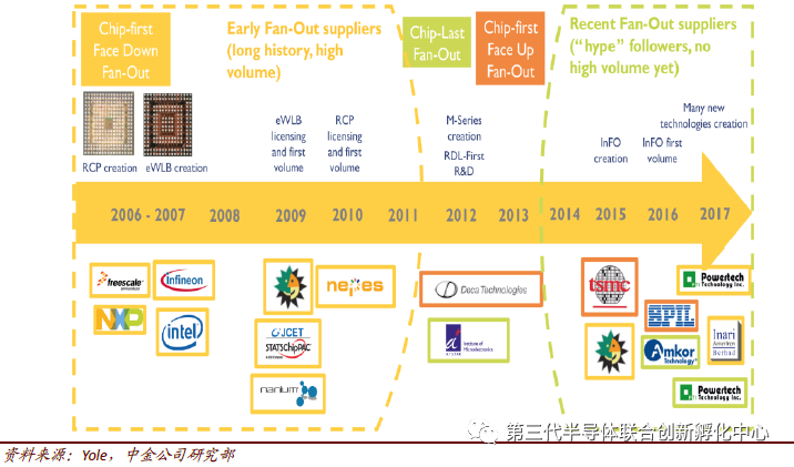
FIWLP and FOWLP serve different purposes, both being mainstream packaging methods for the future. FIWLP is most widely used in analog and mixed-signal chips, followed by wireless interconnects, and CMOS image sensors also adopt FIWLP technology for packaging.
FOWLP will mainly be used in processor chips for mobile devices.
According to Yole’s predictions, before 2018, the main driver for FOWLP was Apple’s smartphone processor chips, and after 2018, the main drivers for FOWLP will include growth in other Android smartphone processors, as well as high-density FOWLP applications in other processing chips, such as AI, machine learning, and IoT.
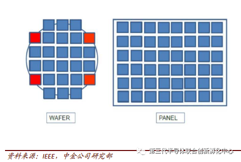
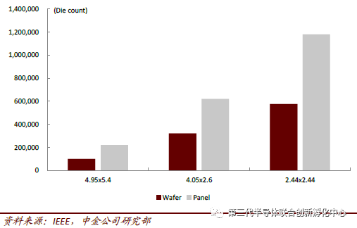
► PLP:Short for Panel-Level Packaging, panel-level packaging is similar to FOWLP, except that the dies are reorganized on a larger rectangular panel instead of a circular wafer.
A larger area means more cost savings and higher packaging efficiency. Additionally, cutting the dies into square shapes avoids area waste that occurs with circular wafer packaging, and rectangular panels effectively solve the waste issue. However, this also raises higher requirements for photolithography and alignment.
▼ Size Comparison of PLP and WLP
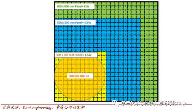
▼ Rectangular Panels Effectively Solve Area Waste
▼ Larger Substrates (600mm x 600mm) Bring Efficiency Improvements
2.5D Packaging: RDL & Interposer
► RDL (Redistribution Layer):At the wafer level, contact redistribution can be performed very efficiently.
The redistribution layer is used to replan the connection paths to the desired areas, achieving higher contact density.
The redistribution process essentially adds one or more layers on top of the original wafer.
First, a dielectric layer is deposited for isolation, then the original contact points are exposed, and a new metal layer is deposited to achieve the new layout.
UBM will be used here to support the solder balls or other contact materials.
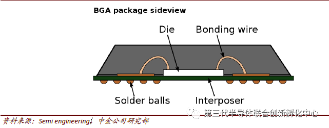
► Interposer:Refers to the conductive layer between solder balls and dies. Its function is to expand the connection surface, redirecting a connection to the desired location, similar to the role of the redistribution layer.
▼ Redistribution Layer (RDL) Illustration

▼ Interposer Illustration
▼ Development Path of Interposer Technology
3D Packaging: TSV, PoP, and MEMS
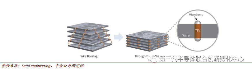
► TSV (Through-Silicon Via):Bump and RDL occupy the planar area where the chip connects to the substrate, while TSV allows chips to be stacked, utilizing three-dimensional space.
More importantly, stacking technology improves electrical properties during multi-chip connections. Wire bonding can be used in stacking technology, but TSV is more attractive.
TSV achieves electrical connections that traverse the entire thickness of the chip, opening the shortest path between the top and bottom surfaces of the chip. Shortening the connection length between chips also means lower power consumption and greater bandwidth.
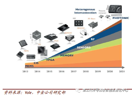
TSV technology was first applied in CMOS image sensors and will be used in fields such as FPGAs, memory, and sensors in the future.
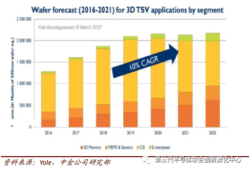
According to Yole, from 2016 to 2021, the number of wafers using TSV technology is expected to grow at a compound annual growth rate of 10%.
3D memory chip packaging will also extensively use TSV in the future.
▼ Evolution Path of 3DIC and TSV Technology
▼ TSV Technology Illustration
▼ Development Path of TSV Technology
▼ TSV Market Size
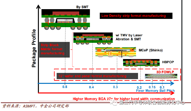
PoP (Package on Package):PoP is a packaging technology that vertically combines separate logic and memory BGA (Ball Grid Array) packages.
In this structure, two or more packaging units are stacked from bottom to top, with a dielectric layer in between to transmit signals. PoP technology increases the integration density of devices, with the bottom packaging unit directly contacting the PCB.
Traditional PoP is based on substrate stacking, and as memory demands higher bandwidth, the spacing between balls requires smaller dimensions, leading to future integration with FOWLP technology for chip-based stacking.
▼ Evolution Trends of PoP Technology
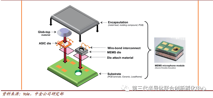
MEMS Packaging:Micro-Electro-Mechanical Systems (MEMS) have seen increasing applications in recent years, with the large-scale deployment of sensors and IoT applications drawing attention to MEMS packaging.
MEMS packaging differs from integrated circuit packaging, with multiple vertical levels including chip-level, module-level, card-level, board-level, and gate-level packaging, requiring consideration of the interactions between different modules during design.
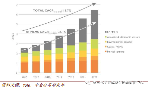
The current MEMS packaging market size is around $2.7 billion, and it is expected to maintain a high growth rate of 16.7% CAGR from 2016 to 2020.
The RFMEMS packaging market is the main driver, with a CAGR of 35.1% from 2016 to 2020.
▼ MEMS Packaging Technology Illustration
In the entire MEMS ecosystem, MEMS packaging is developing rapidly, with wafer-level and 3D integration becoming increasingly important.
The main trend is to develop MEMS manufacturing processes compatible with CMOS for low-temperature wafer bonding and single-chip integration.
Another new trend is the application of bare die stacking in low-cost lead-free semiconductor packaging, which can bring lower costs and smaller pin packages for mass production.
However, the CMOS and 3D integration of MEMS devices pose challenges for modeling, testing, and reliability.
▼ MEMS Packaging Market Forecast
Source:Packaging Testing Laboratory,Shande Semiconductor
-End-
>>>>
Recommended Public Account
>>>>
Distribution Map Collection

 >>>>
>>>>
Join the Community

Previous Reviews
-
Searching for Automotive Grade Power Semiconductor Companies
-
PDF Share | Detailed Explanation of IGBT
-
PDF Share | Chip Packaging
-
PDF Share | Basic Characteristics of IGBT
-
PDF Share | IGBT Illustrated CoursewareAutomotive grade power semiconductor supply chain distribution map, worth collecting!
 【Disclaimer】The article represents the author’s independent views and does not reflect the position of automotive semiconductors. If there are issues regarding the content, copyright, etc., please contact automotive semiconductors at 13866369365 within 30 days of publication for deletion or copyright negotiation.