ClickFollow “Semiconductor New Materials Industry” at the top,Click “❤” and “ ” and share
Addthe editor on WeChat to find like-minded individuals in the industry
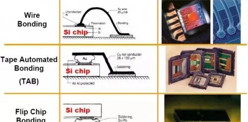
If you have a chip that needs to be fixed onto a circuit board or other substrate to ensure normal output of the chip’s performance, the three most common methods are:
The first method is wire bonding, which connects the chip pins to the circuit using gold wires with good conductivity.
The second method is the Tape Automated Bonding (TAB) technique, which replaces gold wires with copper foil that bonds to the bumps on the chip pins.
The third method is Flip Chip technology, which connects the conductive bumps on the chip to the bumps on the circuit board through a specific process.
As semiconductors become increasingly integrated, smaller, and more powerful, Flip Chip technology is being applied more widely. The Flip Chip process involves directly depositing bumps on the chip’s I/O pads or depositing bumps (including solder balls, lead-free solder balls, copper bumps, and gold bumps) after RDL wiring, flipping the chip, and heating it to combine the molten solder with the substrate or frame, thus completing the required packaging process. A schematic diagram of Flip Chip packaging products is shown below.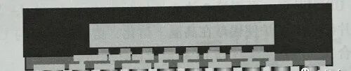 Compared to traditional wire bonding processes, Flip Chip packaging technology has the following advantages:
(1) High VO density.
(2) Due to the use of bump structures, interconnection lengths are greatly shortened, resulting in lower interconnection resistance and inductance, significantly improving the electrical performance of the package.
(3) Heat generated in the chip can be directly transferred to the packaging substrate through the solder bumps, thus reducing the chip temperature.
 Flip Chip technology also places higher demands on packaging processes and reliability for high-density micro bump technology, small pitch Flip Chip bonding technology, and underfill technology. Each process method has its own differences and applications.Today, Flip Chip technology is widely used in consumer electronics, and its applications in the Internet of Things, automotive electronics, and big data will also expand in the future. Flip Chip packaging is considered an essential process for advancing the manufacturing of low-cost, high-density portable electronic devices.
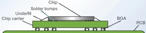 Flip Chip is mainly completed through four steps:
Step 1: Under Bump Metallization (UBM)
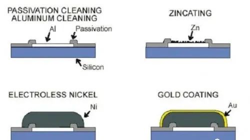 UBM is metallized to extract the performance of the P-N junction in the semiconductor. The most suitable bump material for thermocompression Flip Chip connections is gold, which can be generated through traditional electroplating methods or using the stud bump method, the latter being a common bump formation process in wire bonding technology.
The deposition methods for UBM mainly include:
Sputtering: A thin film is deposited layer by layer on the silicon wafer using sputtering, then a photolithography technique is used to form the UBM pattern, followed by etching away the non-patterned areas.Evaporation: Using a mask, a thin film is deposited layer by layer on the silicon wafer through evaporation. This selective deposition mask can be used for the formation of corresponding bumps.Chemical plating: A selective Ni plating is performed on the Al pads using chemical plating methods. Zincate treatment is often used on the Al surface. This method does not require vacuum or pattern etching equipment, making it low-cost.
Step 2: Bump Formation
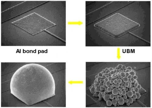 This part is for forming bumps, which can be seen as creating electrodes for the P-N junction, similar to processing an output terminal for a battery.
Common methods for forming bumps include:
Evaporated solder bumps,
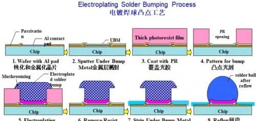
Electroplated solder bumps,
Printed solder bumps,
Stud solder bumps,
Ball bumps,
Solder transfer bumps.
A typical diagram of electroplated solder bumps is shown below:
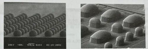
 The completed bumps are observed under a scanning electron microscope, showing a uniform metallic sphere morphology.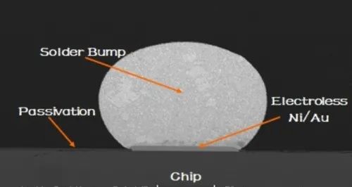
Step 3: Assemble the bumped chip onto the substrate/board
In the thermocompression bonding process, the bumps on the chip are connected to the pads on the substrate through heating and pressing.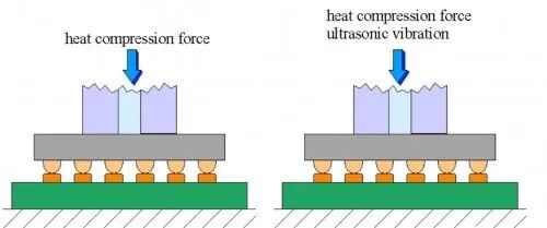
Step 4: Use non-conductive materials to fill the bottom voids of the chip
During filling, the Flip Chip and substrate are heated to 70 to 75°C, and a filler-loaded L-shaped syringe is used to inject the filler bi-directionally along the edges of the chip.
Below is a schematic diagram of the filling process:
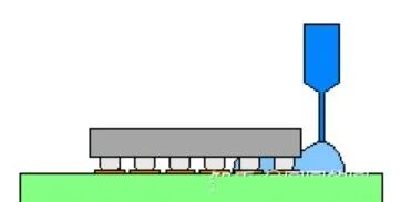 The chip and substrate are stably bonded together after the filling is completed, as shown in the final diagram: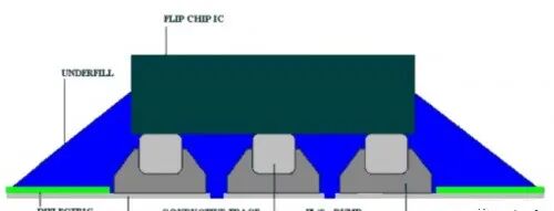
Conclusion
The structure of the Flip Chip from top to bottom consists of a sapphire substrate, N-type semiconductor layer, light-emitting layer, P-type semiconductor layer, and electrodes. Compared to the upright structure, the heat generated at the PN junction in this structure can be directly conducted to the heat sink without passing through the substrate, resulting in good heat dissipation performance, high chip luminous efficiency, and reliability. In the Flip Chip structure, both the p-electrode and n-electrode are located on the bottom surface, avoiding obstruction of the emitted light, thus enhancing the chip’s light output efficiency. Additionally, the distance between the electrodes in the Flip Chip structure is greater, reducing the risk of short circuits caused by metal migration between the electrodes.
- Further reading:Top 10 Chip Companies in China
Global Semiconductor Market Growth: Market Trends for 2025
Global Scale Analysis of Semiconductor Targets (Material Types, Application Analysis, End Users, Major Companies, and Market Outlook)
By 2034, sales of silicon carbide and gallium nitride power semiconductors are expected to soar at a compound annual growth rate of 27.1%
Future Trends and Opportunities in the Global Semiconductor Materials Market
Opportunities and Challenges in the Localization of High-end Photoresists
Acceleration of Localization in China’s Semiconductor Industry
Global Semiconductor Market Forecast (2025-2033)
Two-dimensional Materials Have a Long Way to Go: Global Semiconductor Revenue Expected to Grow by 14% in 2025
How Can Domestic Epoxy Encapsulants Break the Foreign Monopoly and Reshape the Future of Semiconductor Packaging?
What are Semiconductor Materials: Types and Applications Explained
Eight Major Chip Materials in Semiconductors
Who is Shaping the Next Generation of Semiconductor Products with Emerging Materials
Next Generation Semiconductors: A Seven-Year Roadmap for Two-Dimensional Materials; Global Semiconductor Material Market Forecast (2024-2032): Scale, Market Share, Industry Analysis, Types, End Users, Regions
Detailed Illustrated Guide to Silicon Wafer Semiconductor Manufacturing Processes
Main Trends in Semiconductor Packaging and Testing Equipment Market
What are the First, Second, Third, and Fourth Generation Semiconductor Materials?
Semiconductor Market: Top Companies, Emerging Trends, and Future Opportunities
Semiconductor Packaging Market Share and Future Trends
Predictions on Several Factors for Semiconductor Growth in 2025
Unlocking Semiconductor Gold: A Bright Future Ahead
Market Size Analysis of SIC Insulation Films
Market Size Analysis of Advanced Semiconductor Packaging
Key Materials for Semiconductor Packaging – Detailed Explanation of Chip Adhesive Materials
Key Materials for Semiconductor Manufacturing – Detailed Explanation of High-Purity Reagents
Latest Global Semiconductor Company Market Value Rankings as of June 2025 (Including Comparison with January 2025 Global Semiconductor Company Market Value Top 100)
For more information on semiconductors
Welcome to join the Semiconductor Exchange Group
(Group Code: Semiconductor)

【Cooperation and Consultation】 Please scan the QR code to add the editor on WeChat. The editor has been in the materials industry for many years and is always available to discuss material-related questions (please be sure to note your company name when adding).

Click the card below to follow us