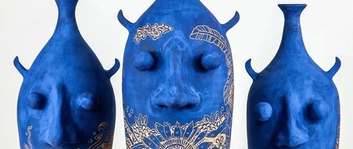
Uart Daily Image | Curves & Tape
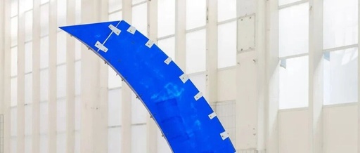
Joost van Bleiswijk Curved and Taped Blue 60x90x170 Aluminium / Hand pigment / painted The studio is Joost’s place for design experimentation, where the creative process often unfolds in a rather instinctive and expressive manner. He is fascinated by and values the process of making, often spending entire days immersed in it, with the sounds … Read more