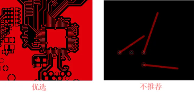
We believe that everyone finds wiring to be an essential part of PCB design, and the rationality of the wiring determines the aesthetics and production costs of the PCB. It also reflects the performance of the circuit and heat dissipation, as well as whether the performance of the components can be optimized.
This article will provide a comprehensive summary of PCB wiring methods.
1. The length of the wiring should include the length of the vias and the package pads.
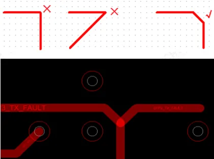
2. The optimal wiring angle is 135°, as any other angle can lead to process issues during PCB fabrication.
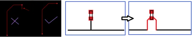
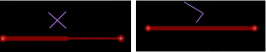
3. Avoid using right angles or acute angles in wiring, as this can cause changes in line width at corners, changes in impedance, and signal reflection, as shown in the figure below.
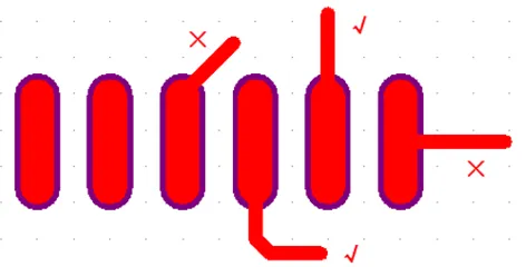
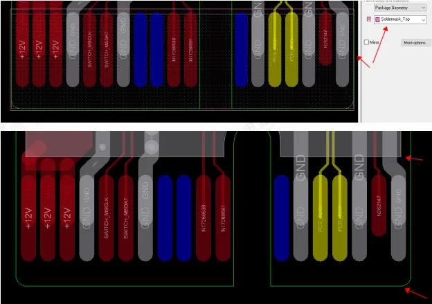
4. Wiring should start from the long side of the pad, avoiding connections from the wide direction or corners of the pad. It is advisable to keep the corners of the wiring at least 6 mil away from the pad, as shown in the figure below.
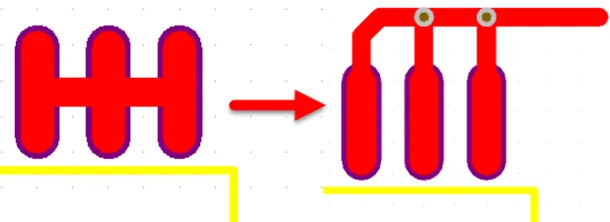
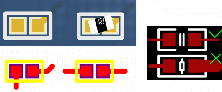
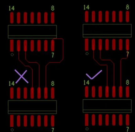
5. As shown in the figure below, adjacent pads on the same network should not be directly connected. They should be connected after leaving the pad, as direct connections can easily lead to solder bridging during hand soldering.
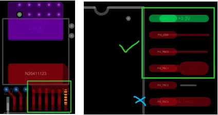
6. For small CHIP devices, pay attention to the symmetry of the wiring, maintaining consistent line widths for both ends. For example, if one pin has copper poured, the other pin should also be treated similarly to reduce component drift and rotation after placement, as shown in the figure below.
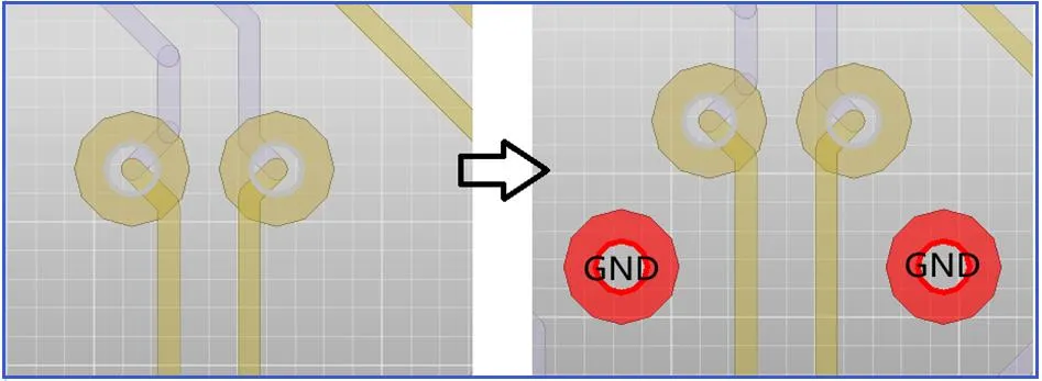
7. For signals that require ground shielding, ensure the integrity of the ground shielding. Try to perform GND hole processing along the ground line, and the distance between two GND holes should not be too far apart, ideally kept within 50-150 mil, as shown in the figure below.
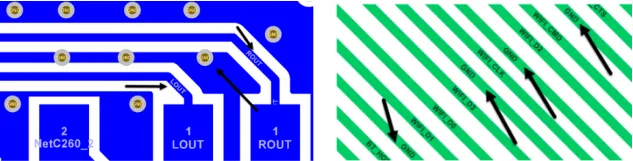
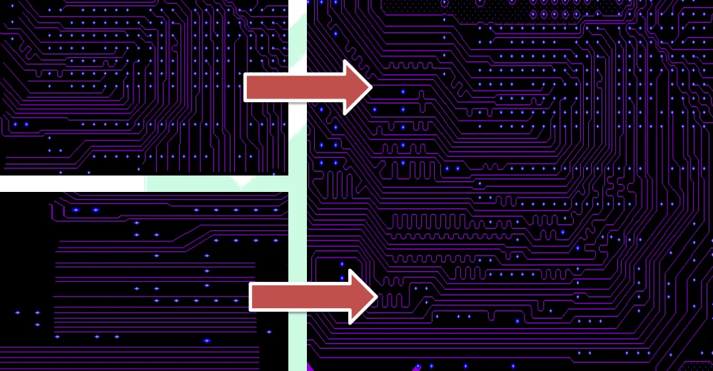
8. The wiring should have a complete and continuous reference layer plane, avoiding high-speed signals crossing areas. It is recommended that high-speed signals be at least 40 mil away from the edge of the reference plane, as shown in the figure below.
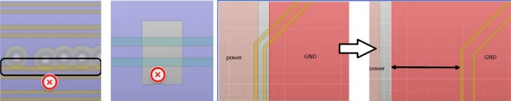
9. Due to the pads of surface-mounted devices causing impedance reduction, to minimize the impact of impedance discontinuity, it is recommended to excavate a layer of reference plane directly below the surface-mounted pads, sized according to the pad size. Common surface-mounted devices include: capacitors, ESD protection, common mode choke inductors, connectors, etc., as shown in the figure below.
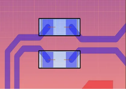
10. As shown in the figure below, the loop area formed by the signal line and its return path should be minimized. A smaller loop area leads to lower radiation and reduced susceptibility to external interference.
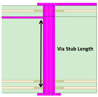
11. As shown in the figure (above), stubs are not allowed in wiring. Try to minimize the length of the stubs, with a recommended length of zero. Avoid via stub effects, especially when the stub length exceeds 12 mil, it is advisable to simulate the impact of via stubs on signal integrity, as shown in the figure (below).
12. Avoid forming self-loops in different layers when routing. This problem often occurs in multilayer board designs, and self-loops can cause radiation interference, as shown in the figure below.
13. It is recommended not to place test points on high-speed signals.
14. For signals that generate interference or are sensitive (such as RF signals), shielding should be planned. The width of the shielding is typically 40 mil (generally kept above 30 mil, can be confirmed with the manufacturing client), and as many GND vias as possible should be added to the shield to enhance its soldering effectiveness.
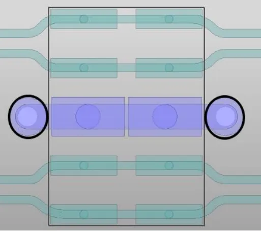
15. The wiring width of the same network should remain consistent. Variations in line width can cause uneven characteristic impedance, leading to reflections at higher transmission speeds. Under certain conditions, such as connector lead wires or BGA packaged lead wires with similar structures, if the spacing is too small, it may not be possible to avoid variations in line width. It is advisable to minimize the effective length of inconsistent sections, as shown in the figure below.
16. The width of the IC pin wiring should be less than or equal to the pad width. The wiring width cannot be greater than the pad width. For some signals that require wider line widths due to current-carrying requirements, the wiring can initially match the pin width and then increase the width by 6-10 mil after leaving the pad, as shown in the figure below.
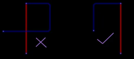
17. The wiring must connect to the center of the pad and via.
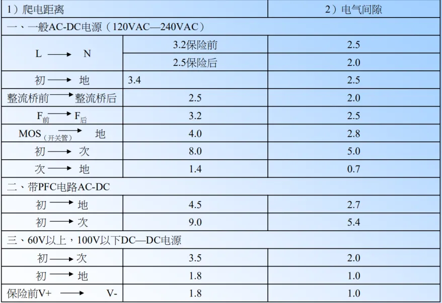
18. For high-voltage signals, ensure the creepage distance, with specific parameters shown in the figure below.
19. For designs that include multiple DDR or other memory chips, confirm the wiring topology with the client and check for any reference documentation.
20. The gold finger area needs to be windowed. In multilayer board designs, all copper layers below the gold finger should be excavated, with the excavation distance from the board frame generally exceeding 3mm.
21. Plan the passage for bottlenecks in advance and reasonably plan the wiring capacity at the narrowest point.
22. Place coupling capacitors as close to the connectors as possible.
23. Series resistors should be placed close to the sending device, while terminating resistors should be placed near the end. For example, series resistors on eMMC clock signals are recommended to be placed near the CPU side (within 400 mil).
24. It is recommended to place a ground via for each ground pad of ICs (such as eMMC chips, FLASH chips, etc.) to effectively shorten the return path, as shown in the figure below.
25. It is recommended that each ground pad of ESD devices has a ground via, and the via should be as close to the pad as possible, as shown in the figure below.
26. Avoid routing near clock devices (such as crystals, oscillators, clock generators, clock distributors), switching power supplies, magnetic devices, and through-hole components.
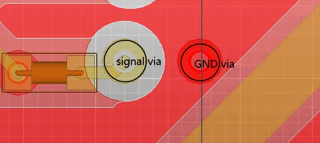
27. When changing layers, and if the reference layers before and after the change are ground planes, place an accompanying via next to the signal via to ensure continuity of the return path. For differential signals, both the signal via and return via should be symmetrically placed, as shown in the figure (above); for single-ended signals, it is recommended to place a return via next to the signal via to reduce crosstalk between vias, as shown in the figure (below).
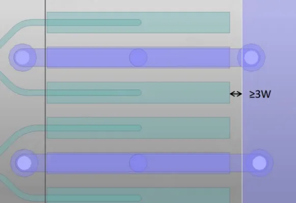
28. The distance between the ground copper of the connector and the signal PAD should be at least three times the line width, as shown in the figure below.
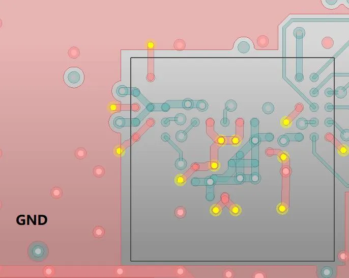
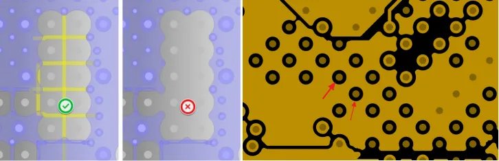
29. In the BGA area, connect using traces or perform pad cutting to avoid damaging the integrity of the plane, as shown in the figure below.
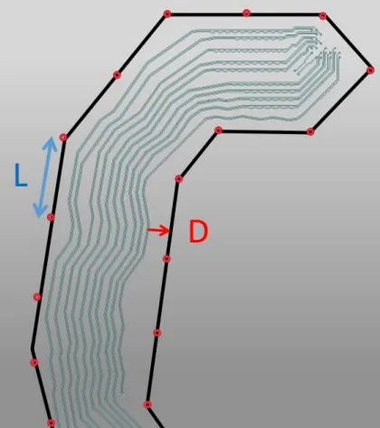
30. When PCB wiring requires ground shielding, the recommended shielding method is shown in the figure below, where L is the spacing between ground line vias, and D is the distance between the ground line and the signal line, suggested to be ≥ 4*W.
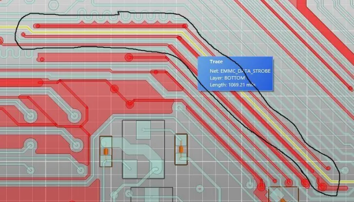
31. Some important high-speed single-ended signals, such as clock signals, reset signals, etc. (like emmc_clk, emmc_datastrobe, RGMII_CLK, etc.), are recommended to be ground shielded. Ground vias should be placed at least every 500 mil along the shielding line, as shown in the figure below.
Disclaimer: The copyright of this article belongs to the original author and does not represent the views of the association. The articles promoted by the “Jiangxi Province Electronic Circuit Industry Association” are for sharing purposes only and do not represent the stance of this account. If there are copyright issues, please contact us for deletion.