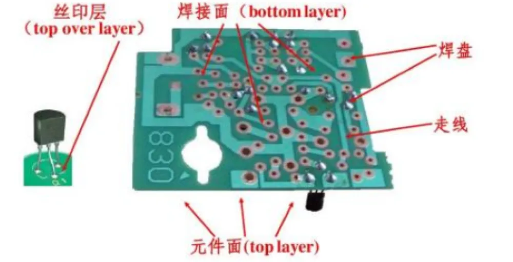
In the design and manufacturing process of PCB boards, engineers need to not only prevent unexpected issues during manufacturing but also avoid design errors. This article summarizes and analyzes these common PCB problems, hoping to provide some assistance for your design and production work.
Problem 1: PCB Short Circuit
This issue is one of the common faults that directly causes the PCB board to malfunction, and there are many reasons for this problem, which we will analyze one by one below.
Beijing Semiconductor Laboratory
The main reason for PCB short circuits is improper pad design. At this time, circular pads can be changed to elliptical ones, increasing the distance between points to prevent short circuits.
Improper design of component orientation on the PCB can also cause short circuits and malfunction. For example, if the pins of SOIC are parallel to the solder wave, it is easy to cause short circuit accidents. In this case, the component orientation can be adjusted to make it perpendicular to the solder wave.
Another possible cause of PCB short circuit faults is bent pins from automatic insertion. Due to IPC regulations that require lead lengths to be less than 2mm and concerns that excessive bending angles may cause components to fall out, this can easily lead to short circuits. Therefore, solder joints should be at least 2mm away from the circuit.
In addition to the three reasons mentioned above, there are other reasons that can also lead to PCB short circuit faults, such as oversized substrate holes, low soldering temperature, poor solderability of the board surface, solder mask failure, and contamination of the board surface. These are common fault causes, and engineers can compare these reasons with the occurrence of faults to systematically eliminate and check them.
Problem 2: Dark and Granular Contacts on PCB
The appearance of dark or granular contacts on the PCB is mostly due to solder contamination and excessive oxides mixed in the solder, resulting in brittle solder joint structures. Care should be taken not to confuse this with darkening caused by using low-tin solder.
Another reason for this problem is changes in the composition of the solder used during processing, with excessive impurities. It may be necessary to add pure tin or replace the solder. Fibrous layering physical changes in the stained glass, such as separation between layers, may occur. However, this condition does not imply poor solder joints. The reason is that the substrate was overheated, requiring a reduction in preheating and solder temperatures or an increase in substrate travel speed.
Problem 3: PCB Solder Joints Turn Gold
Generally, the solder on PCB boards appears silver-gray, but occasionally golden solder joints may appear. The main reason for this problem is excessive temperature, which can be resolved by lowering the soldering furnace temperature.
Problem 4: Poor Board Quality Affected by Environment
Due to the structural reasons of PCB itself, it is very easy to cause damage to the PCB when in unfavorable environments. Extreme temperatures or unpredictable temperature changes, excessive humidity, high-intensity vibrations, and other conditions are factors that lead to reduced performance or even scrapping of the board. For example, changes in environmental temperature can cause deformation of the board, thus damaging solder joints, bending the board shape, or potentially causing the copper traces on the board to break.
On the other hand, moisture in the air can lead to oxidation, corrosion, and rust on metal surfaces, such as exposed copper traces, solder joints, pads, and component leads. Accumulation of dirt, dust, or debris on the surfaces of components and circuit boards can reduce airflow and cooling to components, leading to PCB overheating and performance degradation. Vibration, dropping, striking, or bending the PCB can deform it and lead to cracks, while large currents or overvoltage can cause the PCB to break down or lead to rapid aging of components and pathways.
Problem 5: PCB Open Circuit
When traces break, or solder is only on the pads and not on the component leads, an open circuit occurs. In this case, there is no adhesion or connection between the component and the PCB. Similar to short circuits, these can also occur during the manufacturing process, soldering, and other operations. Vibration or stretching the circuit board, dropping them, or other mechanical deformation factors can damage traces or solder joints. Similarly, chemicals or moisture can lead to wear of solder or metal components, resulting in broken component leads.
Problem 6: Loose or Misaligned Components
During reflow soldering, small components may float on the molten solder and eventually detach from the target solder joint. Possible reasons for misalignment or tilting include insufficient support for the circuit board, reflow oven settings, solder paste issues, and human errors that cause vibrations or bouncing of components soldered on the PCB.
Problem 7: Soldering Issues
The following are some problems caused by poor soldering practices:
Disturbed solder joints: Movement of solder due to external disturbances before solidification. This is similar to cold solder joints but has different causes and can be corrected by re-heating and ensuring that the solder joint is not disturbed during cooling.
Cold solder: This occurs when solder does not melt properly, resulting in rough surfaces and unreliable connections. Excess solder can prevent complete melting, leading to cold solder joints. The remedy is to reheat the joint and remove excess solder.
Solder bridges: This occurs when solder crosses and physically connects two leads together. This can lead to unexpected connections and short circuits, potentially causing components to burn out or traces to break under high current.
Pads: Insufficient wetting of pins or leads. Too much or too little solder. Pads raised due to overheating or rough soldering.
Most defects in PCB manufacturing are caused by human errors. In most cases, incorrect production processes, misplacement of components, and unprofessional manufacturing standards lead to up to 64% of avoidable product defects. The likelihood of defects increases with the complexity of the circuit and the number of production processes due to the following reasons: densely packaged components; multiple circuit layers; fine routing; surface mount components; power and ground planes.
Although every manufacturer or assembler hopes that the produced PCB boards are free of defects, there are always some challenges in the design and production processes that lead to ongoing PCB issues.
Typical problems and results include the following: poor soldering leading to short circuits, open circuits, cold solder joints, etc.; misalignment of board layers leading to poor contact and overall performance; poor insulation of copper traces leading to arcing between traces; placing copper traces too close to pathways increases the risk of short circuits; insufficient thickness of the circuit board can lead to bending and breaking.
Statement:The copyright of this article belongs to the original author and does not represent the views of the association.The articles promoted by the “Jiangxi Province Electronic Circuit Industry Association” are for sharing purposes only and do not represent this account’s position. If there are copyright issues, please contact us for deletion.