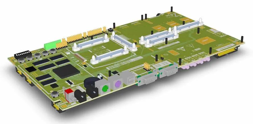
Click the “Mechanical and Electronic Engineering Technology” above to follow usYour smartphone, computer, smartwatch, and even the smart socket and router at home are all high-tech products whose core component is the PCB, or printed circuit board. Without it, these devices cannot perform their various complex functions. So, what exactly is PCB design? Why is it so important? Today, let’s unveil the mystery of PCB design together.Imagine if you were a chef preparing a sumptuous feast; you would need various ingredients, seasonings, and a clean, tidy kitchen. Similarly, in the world of electronic products, the PCB is that “kitchen.” It cleverly combines all electronic components, circuits, and interfaces to form a functioning system. PCB design is about how to cleverly plan the layout of this “kitchen,” ensuring that all the “ingredients” can coexist harmoniously and achieve the best results.In PCB design, a very important concept is “layers.” Imagine you have a multi-layer cake, with each layer having different flavors and decorations. In a PCB, these “layers” represent different routing layers, power layers, ground layers, etc. Each layer has its specific function, and they work together to ensure the entire circuit board operates normally. For example, the power layer provides electricity, the ground layer returns current, and the signal routing layer transmits various signals. These layers are like hidden “rooms” within the PCB, interconnected by vias, just like chocolate sticks in a cake, tightly linking each layer together.Speaking of vias, this is a small trick in PCB design. Don’t underestimate its size; it plays a significant role. It acts like a “bridge” in the circuit, connecting different layers and allowing current and signals to flow smoothly. However, one must not be careless when designing vias. Too many vias can affect the performance and reliability of the circuit board, while too few may not suffice. Therefore, designers must carefully calculate to ensure that each via is just right. Moreover, the size and position of the vias must be meticulously designed; otherwise, they may affect surrounding components and circuits.In addition to vias, the silk screen layer is also an essential part of PCB design. The silk screen layer acts like the “instruction manual” of the circuit board, marking various components’ names, numbers, orientations, and other information. This information is crucial for the installation, maintenance, and debugging of the circuit. Imagine if you bought a new appliance, but the manual had nothing written in it; wouldn’t that be frustrating? Similarly, if there is no silk screen layer on the PCB, maintenance and debugging would be very challenging. Therefore, designers must ensure that the information is accurate and visually appealing, making it easy to understand at a glance when designing the silk screen layer.When it comes to components, we must mention SMD (Surface Mount Devices). SMD is a very compact component that can be directly soldered onto the surface of the circuit board without the need for through-hole like traditional plug-in components. The advent of SMD has greatly improved the integration and reliability of circuit boards but also presents new challenges for designers. Because SMD is very small, designers must be particularly careful during the design process to avoid losing pins or placing components in the wrong position. Once soldered, it becomes very difficult to remove them. Therefore, designers must use specialized software to simulate and check, ensuring that each component is placed correctly during the design process.In PCB design, there is also a concept that can be easily confused: the difference between grid fill areas and fill areas. These two terms sound similar, but there are significant differences in computing. A grid fill area is composed of many small squares, resembling a dense net. In contrast, a fill area is a complete area without grid-like segmentation. There are also some differences in usage. For example, when auto-routing, grid fill areas may complicate the routing, while fill areas are relatively simpler. Therefore, designers must choose the appropriate method based on actual needs during the design process.Pads are also an indispensable part of PCB design. Pads are the “interfaces” where components connect with the circuit board, and their quality directly affects the soldering quality and reliability of the components. Therefore, designers must consider many factors when designing pads, such as the shape, size, and arrangement of components. Different components require different pad shapes and sizes, and the distance between pads must also be just right. Otherwise, if problems arise during soldering, it could lead to the entire circuit board being scrapped. Thus, designers must be particularly careful when designing pads, ensuring that each pad meets the requirements.During PCB production, various films are also used, such as solder mask and anti-solder mask. These films play a very important role in the PCB production process. The solder mask helps components solder better to the circuit board, while the anti-solder mask prevents current and signals from flowing in undesired areas. The setup and adjustment of these films are also part of PCB design. Designers must choose the appropriate films based on actual needs and ensure that their thickness, position, and size are just right.Finally, let’s talk about flying leads. In PCB design, flying leads have two meanings. One is the temporary lines automatically generated by the software based on the connection relationships between components before auto-routing. These lines are like kite strings in the sky, tightly linking various components together. Designers can observe these flying leads to adjust component positions and routing strategies, making the circuit board more aesthetically pleasing and practical. The other type of flying lead is when, during mass automated production, flying leads are treated as resistive components with uniform pad spacing for design. This design can greatly improve production efficiency and quality but also requires designers to possess rich experience and skills.After discussing so much, you may have gained a certain understanding of PCB design. However, this is just the tip of the iceberg. PCB design is a complex and meticulous process that involves a lot of specialized knowledge and skills. Designers need to continuously learn and explore to create better and more reliable circuit boards.