Skip to content
Today, we will discuss the key points to consider when designing a PCB from a soldering perspective.
1. Factors Affecting PCB Soldering Quality
From PCB design to the completion of soldering all components, achieving a high-quality circuit board requires the control of various aspects including PCB engineers, soldering processes, and soldering workers.
The main influencing factors include: PCB diagrams, the quality of the circuit board, the quality of components, the degree of oxidation of component pins, the quality of solder paste, the printing quality of solder paste, the accuracy of programming for the pick-and-place machine, the placement quality of the pick-and-place machine, the temperature curve of the reflow oven, and so on.
The aspect that the soldering factory cannot surpass is the PCB drawing.
People who design circuits rarely solder circuit boards and thus lack rich soldering experience, while workers in soldering factories do not understand board design and are solely focused on completing production tasks without the time or ability to analyze the causes of poor soldering.
These two types of talents serve their respective roles but find it difficult to integrate organically.
2. Suggestions for PCB Drawing
Here are some suggestions to avoid various poor drawing methods that affect soldering quality.
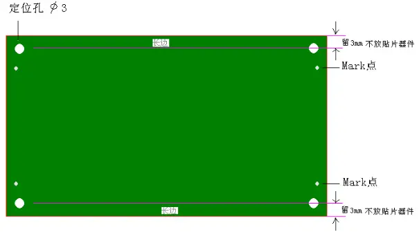
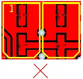
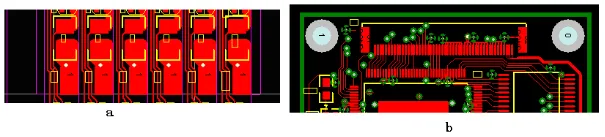
1. Regarding Positioning Holes
The four corners of the PCB should have four holes (minimum diameter 2.5mm) for positioning the circuit board during solder paste printing. The centers in the X-axis or Y-axis direction should be aligned as shown below:
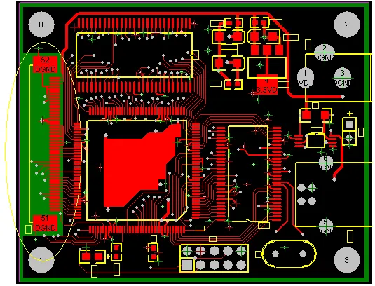
Mark points should be indicated on the PCB for positioning by the pick-and-place machine.
Specific location: diagonally opposite corners of the board, which can be circular or square pads, and should not be mixed with other component pads. If there are components on both sides, both sides should be marked.
Consider adding MARK points on the panel as well.
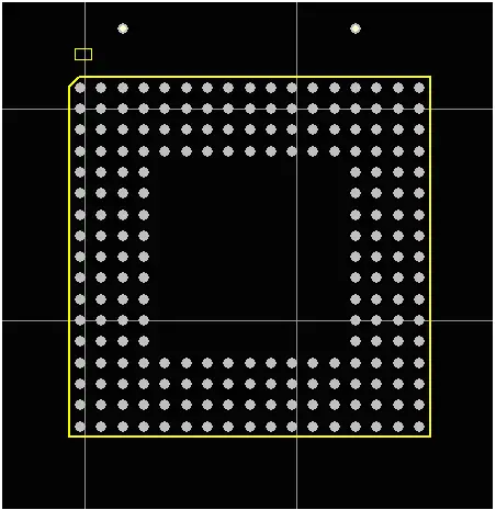
3. When Designing PCBs, Please Note the Following Points:
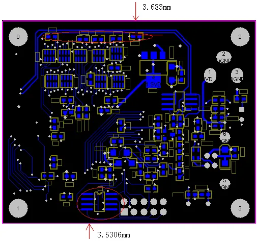
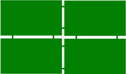
a. The shape of the Mark point should refer to the pattern shown below, either vertically or horizontally symmetrical.
b. The size of A should be 2.0mm.
c. There should not be any shapes or color variations within a 2.0mm range from the outer edge of the Mark point that could cause misidentification (pads, solder paste).
d. The color of the Mark point should have a contrast with the surrounding PCB color.
e. To ensure recognition accuracy, the surface of the Mark point should be electroplated with copper or tin to prevent reflection. Marks that are only lines cannot be recognized.
As shown in the figure below:
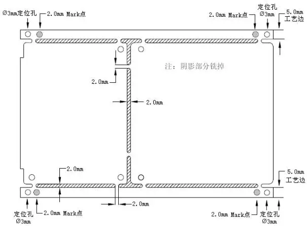
4. About Leaving a 5mm Margin
When drawing PCBs, a margin of at least 3mm should be left in the long edge direction for the pick-and-place machine to transport the circuit board. No components should be placed within this range.
For double-sided components, consider issues such as components being knocked off or pads being scraped during secondary reflow soldering.
It is recommended not to place components in the 5mm margin on the longer side where there are fewer chips. If limited by the PCB area, processing edges can be done on the long side.
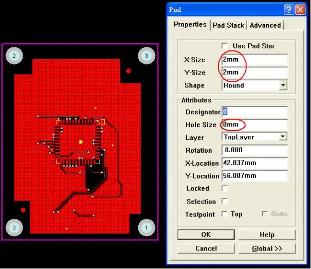
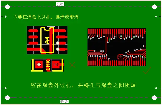
5. Do Not Drill Holes Directly on Pads
Drilling holes on pads can cause solder paste to flow into the holes during reflow soldering, leading to missing solder on component pads and causing cold solder joints, as shown in the figure below.
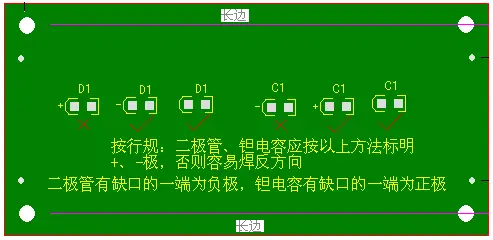
 6. Regarding the Polarity Marking of Diodes and Tantalum Capacitors
The polarity marking of diodes and tantalum capacitors should comply with industry standards to prevent workers from soldering in the wrong direction based on experience. As shown in the figure:
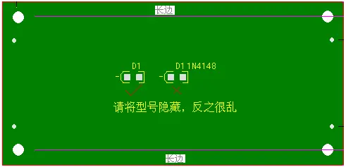
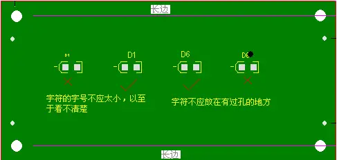
7. Regarding Silkscreen and Markings
Please hide the component model, especially on densely populated circuit boards. Otherwise, the clutter can hinder finding soldering positions. As shown in the figure:
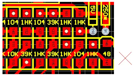
Do not only indicate the model without marking the number. As shown in the figure, this can cause issues during programming the pick-and-place machine.
The font size of the silkscreen characters should not be too small, and the placement of characters should avoid overlapping with holes to prevent misreading.
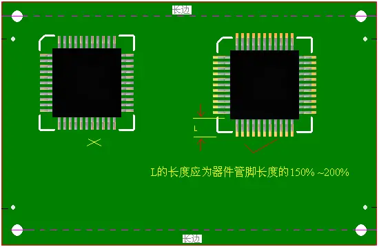
8. Regarding Extending IC Pads
For ICs with SOP, PLCC, QFP, etc., the length of the pads on the PCB should equal the length of the IC pins multiplied by 1.5 for easier hand soldering, allowing the chip pins to merge with the PCB pads and solder. As shown in the figure:
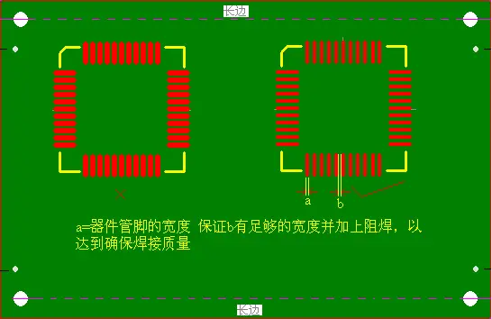
9. Regarding the Width of IC Pads
For ICs with SOP, PLCC, QFP, etc., when drawing PCBs, attention should be paid to the width of the pads. The width of pad a on the PCB should equal the width of the IC pins (Nominal value in the datasheet), and widening is not recommended to ensure that the spacing b between two pads is sufficient to avoid bridging. As shown in the figure:
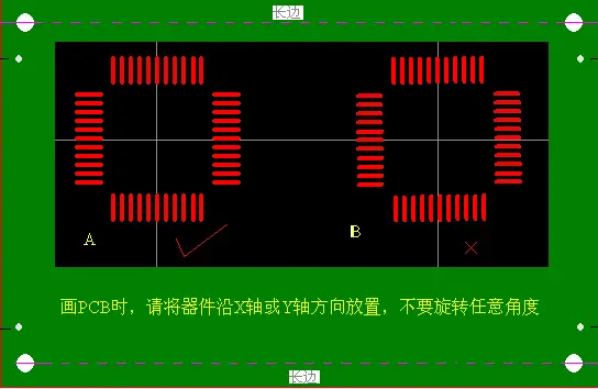
10. Do Not Rotate Components at Arbitrary Angles
Since the pick-and-place machine cannot rotate at arbitrary angles, it can only rotate at 90°, 180°, 270°, and 360°.
As shown in the figure, if component B is rotated 1°, after placement, the component pins will be misaligned with the pads on the circuit board by 1°, thus affecting soldering quality.
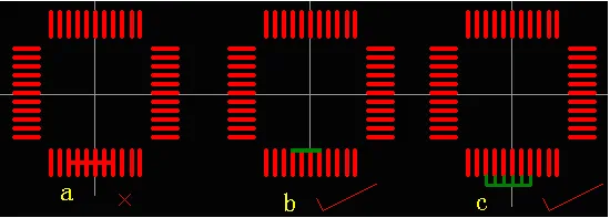
11. Issues to Note When Short-Circuiting Adjacent Pins
The short-circuiting method in Figure a is not conducive to worker recognition and is unsightly after soldering.
If the short-circuiting is done according to methods b and c in the drawing and solder mask is added, the soldering effect will be different.
As long as each pin is not connected, there will be no short circuit phenomenon for that chip, and it will also look aesthetically pleasing.
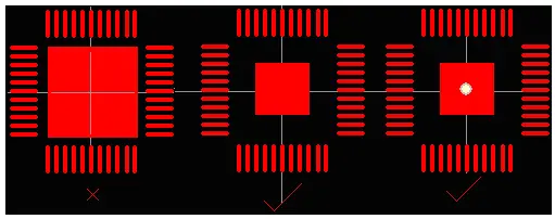
12. Regarding the Middle Pad Under Chips
For chips with a belly shape, it is recommended to reduce the size of the middle pad to increase the distance from the surrounding pads and reduce the chances of short circuits. As shown in the figure:
13. Do Not Place Two Thick Components Too Close Together
As shown in the figure, such a layout can cause the pick-and-place machine to hit the previously placed component when placing the second component, resulting in the machine detecting a danger and shutting down automatically.
Due to the special nature of BGA packaging, its pads are underneath the chip, making it impossible to see the soldering effect.
To facilitate rework, it is recommended to drill two positioning holes of size 30mil on the PCB for positioning the stencil during rework.
Note: The size of the positioning holes should not be too large or too small, allowing the pins to fit snugly without falling or wobbling during insertion, otherwise, positioning will be inaccurate. As shown in the figure:
It is recommended not to use red color. Red PCBs appear white under the red light source of the pick-and-place machine’s camera, making programming difficult and inconvenient for soldering.
16. Regarding Small Components Under Large Components
Some people like to place small components under larger components on the same layer, for example, placing resistors under digital tubes, as shown in the figure:
This layout can complicate rework, as the digital tube must be removed first during rework, which may damage the digital tube. It is recommended to place the resistors under the digital tubes on the bottom side, as shown in the figure:
17. Regarding the Connection of Copper Coating and Pads Affecting Solder Melting
Due to copper coating absorbing a large amount of heat, solder may not melt sufficiently, leading to cold solder joints, as shown in the figure:
In Figure a, the component pad is directly connected to the copper coating; in Figure b, the 50-pin connector is not directly connected to the copper coating, but due to the large area of copper coating in the middle two layers of a four-layer board, both figures a and b will have solder paste that cannot melt sufficiently due to the copper coating absorbing a large amount of heat.
In Figure b, the body of the 50-pin connector is made of plastic that is not heat resistant. If the temperature is set too high, the connector body will melt or deform; if the temperature is set too low, the copper coating will absorb a large amount of heat and prevent the solder paste from melting sufficiently. Therefore, it is recommended to isolate pads from large areas of copper coating, as shown in the figure:
18. Suggestions for Panelization and Processing Edges
Nowadays, there are more and more engineers who can use software to draw, design, and route PCBs. Completing the design and improving soldering efficiency requires attention to the above elements.
Cultivating good drawing habits and being able to communicate well with processing plants is something every engineer should consider.
Disclaimer: This article is copyrighted by the original author and does not represent the views of the association. The articles shared by the “Jiangxi Province Electronic Circuit Industry Association” are for sharing purposes only and do not represent the stance of this account. If there are copyright issues, please contact us for deletion.
6. Regarding the Polarity Marking of Diodes and Tantalum Capacitors
The polarity marking of diodes and tantalum capacitors should comply with industry standards to prevent workers from soldering in the wrong direction based on experience. As shown in the figure:
7. Regarding Silkscreen and Markings
Please hide the component model, especially on densely populated circuit boards. Otherwise, the clutter can hinder finding soldering positions. As shown in the figure:
Do not only indicate the model without marking the number. As shown in the figure, this can cause issues during programming the pick-and-place machine.
The font size of the silkscreen characters should not be too small, and the placement of characters should avoid overlapping with holes to prevent misreading.
8. Regarding Extending IC Pads
For ICs with SOP, PLCC, QFP, etc., the length of the pads on the PCB should equal the length of the IC pins multiplied by 1.5 for easier hand soldering, allowing the chip pins to merge with the PCB pads and solder. As shown in the figure:
9. Regarding the Width of IC Pads
For ICs with SOP, PLCC, QFP, etc., when drawing PCBs, attention should be paid to the width of the pads. The width of pad a on the PCB should equal the width of the IC pins (Nominal value in the datasheet), and widening is not recommended to ensure that the spacing b between two pads is sufficient to avoid bridging. As shown in the figure:
10. Do Not Rotate Components at Arbitrary Angles
Since the pick-and-place machine cannot rotate at arbitrary angles, it can only rotate at 90°, 180°, 270°, and 360°.
As shown in the figure, if component B is rotated 1°, after placement, the component pins will be misaligned with the pads on the circuit board by 1°, thus affecting soldering quality.
11. Issues to Note When Short-Circuiting Adjacent Pins
The short-circuiting method in Figure a is not conducive to worker recognition and is unsightly after soldering.
If the short-circuiting is done according to methods b and c in the drawing and solder mask is added, the soldering effect will be different.
As long as each pin is not connected, there will be no short circuit phenomenon for that chip, and it will also look aesthetically pleasing.
12. Regarding the Middle Pad Under Chips
For chips with a belly shape, it is recommended to reduce the size of the middle pad to increase the distance from the surrounding pads and reduce the chances of short circuits. As shown in the figure:
13. Do Not Place Two Thick Components Too Close Together
As shown in the figure, such a layout can cause the pick-and-place machine to hit the previously placed component when placing the second component, resulting in the machine detecting a danger and shutting down automatically.
Due to the special nature of BGA packaging, its pads are underneath the chip, making it impossible to see the soldering effect.
To facilitate rework, it is recommended to drill two positioning holes of size 30mil on the PCB for positioning the stencil during rework.
Note: The size of the positioning holes should not be too large or too small, allowing the pins to fit snugly without falling or wobbling during insertion, otherwise, positioning will be inaccurate. As shown in the figure:
It is recommended not to use red color. Red PCBs appear white under the red light source of the pick-and-place machine’s camera, making programming difficult and inconvenient for soldering.
16. Regarding Small Components Under Large Components
Some people like to place small components under larger components on the same layer, for example, placing resistors under digital tubes, as shown in the figure:
This layout can complicate rework, as the digital tube must be removed first during rework, which may damage the digital tube. It is recommended to place the resistors under the digital tubes on the bottom side, as shown in the figure:
17. Regarding the Connection of Copper Coating and Pads Affecting Solder Melting
Due to copper coating absorbing a large amount of heat, solder may not melt sufficiently, leading to cold solder joints, as shown in the figure:
In Figure a, the component pad is directly connected to the copper coating; in Figure b, the 50-pin connector is not directly connected to the copper coating, but due to the large area of copper coating in the middle two layers of a four-layer board, both figures a and b will have solder paste that cannot melt sufficiently due to the copper coating absorbing a large amount of heat.
In Figure b, the body of the 50-pin connector is made of plastic that is not heat resistant. If the temperature is set too high, the connector body will melt or deform; if the temperature is set too low, the copper coating will absorb a large amount of heat and prevent the solder paste from melting sufficiently. Therefore, it is recommended to isolate pads from large areas of copper coating, as shown in the figure:
18. Suggestions for Panelization and Processing Edges
Nowadays, there are more and more engineers who can use software to draw, design, and route PCBs. Completing the design and improving soldering efficiency requires attention to the above elements.
Cultivating good drawing habits and being able to communicate well with processing plants is something every engineer should consider.
Disclaimer: This article is copyrighted by the original author and does not represent the views of the association. The articles shared by the “Jiangxi Province Electronic Circuit Industry Association” are for sharing purposes only and do not represent the stance of this account. If there are copyright issues, please contact us for deletion.