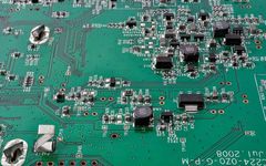
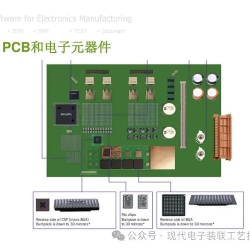
PCB Circuit Board Manufacturing Process Display
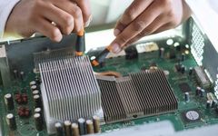
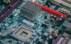
☞ This is the 17006th article published by Metal Processing (mw1950pub). Editor’s Note The production of PCB is very complex. Taking a four-layer printed circuit board as an example, the manufacturing process mainly includes PCB layout, core board production, inner layer PCB layout transfer, core board drilling and inspection, lamination, drilling, copper chemical deposition on … Read more