The execution modes of FPGA are download mode and programming mode.
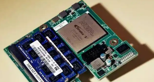
1. FPGA is a type of digital integrated circuit chip, known as “Field Programmable Gate Array”. An important feature of FPGA is its programmability, which allows users to specify a particular digital circuit through programming. The components of FPGA include CLB (Configurable Logic Block), IOB (Input/Output Block), programmable interconnect resources, SRAM, DSP, and clock management modules. The CLB contains Flip-Flops and LUTs, which can implement certain combinational or sequential logic circuits; the IOB is connected to the chip pins and contains circuits such as buffers and tri-state gates.
2. FPGA uses a Logic Cell Array (LCA), which includes configurable logic modules (CLB), input/output modules (IOB), and internal wiring. FPGA can serve as a prototype for fully customized or semi-custom ASIC circuits. It employs high-speed CHMOS technology, has low power consumption, and can be compatible with CMOS and TTL levels.
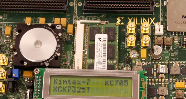
3. The parallel master mode involves one FPGA and one EPROM, while the master-slave mode can support programming multiple FPGAs with one PROM. The serial mode can use a serial PROM to program the FPGA. Utilizing a 65nm process, it can provide up to 330,000 logic units, 1,200 I/Os, and a large number of hard IP blocks, integrating more logic functions, DSP, embedded processing, and interface modules for different applications, which also complicates clock management and voltage distribution issues.