Route according to the 50-ohm impedance line width, try to route from the center of the pad, keeping the lines straight and preferably on the top layer. When a bend is necessary, make it at a 45-degree angle or as an arc, preferably bending near capacitors or resistors. If routing meets the matching requirements of components, strictly follow the reference length values in the datasheet. For example, the routing length between an amplifier and a capacitor (or between inductors) must be adhered to.
1. General Practices
When designing PCBs, to make high-frequency circuit boards more reasonable and improve anti-interference performance, the following aspects should be considered:
(1) Reasonable Layer Selection: In PCB design for high-frequency circuit board routing, using the inner layers as power and ground planes can provide shielding, effectively reduce parasitic inductance, shorten signal line lengths, and decrease cross-interference between signals.
(2) Routing Method: Routing must be done with 45-degree angles or arcs to minimize the emission of high-frequency signals and coupling between them.
(3) Routing Length: The shorter the routing length, the better; the closer the parallel lines, the better.
(4) Number of Vias: The fewer vias, the better.
(5) Inter-layer Routing Direction: The routing direction between layers should be perpendicular, with the top layer being horizontal and the bottom layer being vertical, to reduce interference between signals.
(6) Copper Pouring: Increasing ground copper pour can reduce interference between signals.
(7) Grounding: Grounding important signal lines can significantly enhance their anti-interference capability, and grounding interference sources can prevent them from affecting other signals.
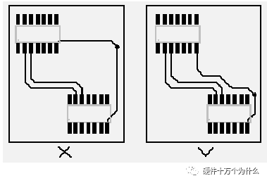
(8) Signal Lines: Signal routing should not form loops and should follow a daisy chain layout.
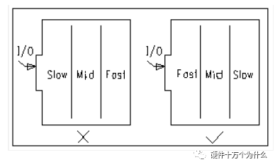
2. Routing Priority
Prioritize critical signal lines: Analog small signals, high-speed signals, clock signals, and synchronous signals should be routed first. Density priority principle: Start routing from the most complex connections on the board. Begin routing from the densest areas on the board. Notes: a. Provide dedicated routing layers for clock signals, high-frequency signals, and sensitive signals, ensuring minimal loop area. If necessary, manual routing, shielding, and increased safety spacing should be employed to ensure signal quality. b. The EMC environment between power and ground layers is poor, so avoid placing interference-sensitive signals. c. Networks with impedance control requirements should be routed according to line length and width requirements.
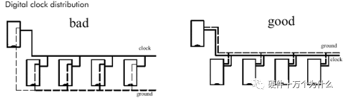
3. Clock Routing
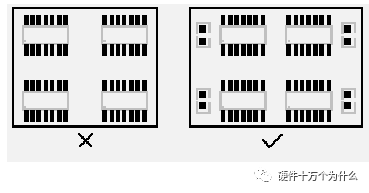
Clock lines are one of the factors that have the greatest impact on EMC. Minimize vias on clock lines, avoid parallel routing with other signal lines, and keep them away from general signal lines to prevent interference. Also, avoid routing near the power section of the board to prevent mutual interference between power and clock signals. If there is a dedicated clock generation chip on the board, no routing should be done beneath it; copper should be poured underneath, and grounding may be necessary. For many chips with reference crystal oscillators, no routing should be done beneath these oscillators, and copper should be poured for isolation.
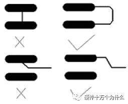
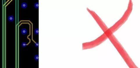
4. Right Angle Routing
Right angle routing is generally to be avoided in PCB routing and has almost become one of the standards for measuring routing quality. So how much impact does right angle routing have on signal transmission? Theoretically, right angle routing causes changes in the transmission line width, resulting in impedance discontinuity. In fact, not only right angles but also sharp angles can cause impedance variations. The impact of right angle routing on signals is mainly reflected in three aspects: first, corners can be equivalent to capacitive loads on the transmission line, slowing down the rise time; second, impedance discontinuity can cause signal reflections; third, sharp corners can generate EMI.
5. Sharp Angles
(1) For high-frequency currents, when the wire bends at right angles or sharp angles, the magnetic flux density and electric field strength near the corner are relatively high, radiating strong electromagnetic waves, and the inductance at this point is larger than that at obtuse or rounded corners.
(2) For digital circuit bus routing, using obtuse or rounded corners occupies less area. Under the same line spacing conditions, the total width occupied by the line spacing is 0.3 times less than that of right angle bends.
6. Differential Routing
Refer to: Differential Routing and Impedance Matching
Differential signals are increasingly used in high-speed circuit design, and the most critical signals in circuits often adopt differential structure design. Definition: Simply put, the driver sends two equal and opposite signals, and the receiver determines the logic state of “0” or “1” by comparing the difference between these two voltages. The pair of lines carrying differential signals is called differential routing.
Compared to ordinary single-ended signal routing, differential signals have the most obvious advantages in the following three aspects: a. Strong anti-interference capability, as the coupling between the two differential lines is good; when external noise interference exists, it is almost simultaneously coupled to both lines, and the receiver only cares about the difference between the two signals, so external common-mode noise can be completely canceled out. b. Effective suppression of EMI; similarly, due to the opposite polarities of the two signals, the electromagnetic fields they radiate can cancel each other out, and the tighter the coupling, the less electromagnetic energy is radiated to the outside. c. Precise timing positioning; since the switching changes of differential signals occur at the intersection of the two signals, unlike ordinary single-ended signals that rely on high and low threshold voltages for judgment, they are less affected by process and temperature, reducing timing errors, and are also more suitable for low-amplitude signal circuits. Currently popular LVDS (low voltage differential signaling) refers to this small amplitude differential signal technology.
For PCB engineers, the main concern is how to ensure that the advantages of differential routing can be fully realized in actual routing. Anyone who has dealt with layout will understand the general requirements for differential routing, which are “equal length, equal spacing.” Equal length is to ensure that the two differential signals always maintain opposite polarities, reducing common-mode components; equal spacing is mainly to ensure that the differential impedance of both is consistent, reducing reflections. The “as close as possible principle” is sometimes also a requirement for differential routing.
7. Serpentine Routing
Serpentine routing is a commonly used routing method in layout. Its main purpose is to adjust the delay to meet system timing design requirements. Designers must first recognize that serpentine routing can degrade signal quality and alter transmission delays, so it should be avoided as much as possible. However, in practical design, to ensure that signals have sufficient hold time or to reduce timing offsets between signals in the same group, it is often necessary to deliberately use serpentine routing.
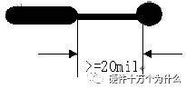
Notes: Paired differential signal lines should generally be routed in parallel, minimizing vias; if vias are necessary, they should be done together for both lines to achieve impedance matching. Groups of signals with the same attributes should be routed side by side to maintain equal length. Vias from surface mount pads should be kept as far from the pads as possible.
9. Power and Ground Line Handling
Even if the routing throughout the PCB is well done, interference caused by inadequate consideration of power and ground lines can degrade product performance and sometimes even affect product success rates. Therefore, the routing of power and ground lines must be taken seriously to minimize noise interference generated by them, ensuring product quality.
Every engineer involved in electronic product design understands the causes of noise between ground and power lines. Here, we will only discuss methods to reduce noise suppression:
(1) It is well known to add decoupling capacitors between power and ground lines. (2) Try to widen the power and ground line widths, preferably making the ground line wider than the power line. Their relationship is: ground line > power line > signal line. Typically, the signal line width is 0.2-0.3mm, with the thinnest width reaching 0.05-0.07mm, while the power line is 1.2-2.5mm. For digital circuit PCBs, a wide ground conductor can form a loop, constituting a ground network (this cannot be done for analog circuit grounds). (3) Use large copper areas as ground; connect all unused areas on the printed board to ground. Alternatively, use multilayer boards, with power and ground each occupying one layer.
In areas with dense vias, avoid connecting vias in the power and ground layer’s cutout areas, which can disrupt the integrity of the plane layer and increase the loop area of signal lines in the ground layer.
Ground loop rules:
The minimum loop rule states that the area of the loop formed by the signal line and its return path should be as small as possible; the smaller the loop area, the less radiation to the outside and the less interference received from the outside.
Decoupling rules for components:
A. Add necessary decoupling capacitors on the printed circuit board to filter out interference signals on the power supply, stabilizing the power supply signal. In multilayer boards, the position of decoupling capacitors is generally not too high, but in double-layer boards, the layout of decoupling capacitors and the routing of power will directly affect the stability of the entire system, sometimes even determining the success or failure of the design. B. In double-layer board design, the current should first pass through filtering capacitors before being supplied to components. C. In high-speed circuit design, the correct use of decoupling capacitors is crucial for the stability of the entire board.
10. Common Ground Handling for Digital and Analog Circuits
Many PCBs are no longer single-function circuits (digital or analog) but are composed of mixed digital and analog circuits. Therefore, when routing, it is necessary to consider the interference issues between them, especially noise interference on the ground.
Digital circuits operate at high frequencies, while analog circuits are highly sensitive. For signal lines, high-frequency signal lines should be kept as far away as possible from sensitive analog circuit components. For ground lines, the PCB should only have one node to the outside, so the common ground issue between digital and analog must be handled internally on the PCB. Internally, the digital ground and analog ground are actually separated and not connected, only at the interface connecting the PCB to the outside (such as connectors). There should be only one connection point between digital and analog grounds. There are also cases where the PCB does not share a ground, which is determined by system design.
11. Signal Lines Routed on Power (Ground) Layers
In multilayer printed boards, if there are few remaining lines to be routed on the signal layer, adding more layers will cause waste and increase production workload, thus increasing costs. To resolve this conflict, consider routing on the power (ground) layers. First, consider using the power layer, and then the ground layer, as it is best to maintain the integrity of the ground layer.
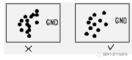
12. Handling of Connection Legs in Large Area Conductors
In large area grounds (or power), the handling of connection legs of commonly used components requires comprehensive consideration. In terms of electrical performance, it is best for the component leg pads to be fully connected to the copper surface, but this poses some potential issues for component soldering assembly, such as:① Soldering requires high-power heaters.② It is easy to create cold solder joints.Therefore, balancing electrical performance and process needs, a cross-shaped pad is made, known as thermal isolation (heat shield), commonly referred to as thermal pads, which greatly reduces the likelihood of cold solder joints caused by excessive heat dissipation during soldering. The same handling applies to the connection legs of the power (ground) layers in multilayer boards.
13. The Role of Network Systems in Routing
In many CAD systems, routing is determined by the network system. A dense grid increases pathways, but if the steps are too small, the data volume of the drawing will be too large, which will inevitably require higher storage space for the equipment and significantly impact the computational speed of electronic products. Some pathways are ineffective, such as those occupied by component leg pads or installation holes. A sparse grid with too few pathways greatly affects routing efficiency. Therefore, a reasonably dense grid system is needed to support routing.
The standard distance between two legs of standard components is 0.1 inches (2.54mm), so the basic grid system is generally set to 0.1 inches (2.54mm) or multiples less than 0.1 inches, such as 0.05 inches, 0.025 inches, 0.02 inches, etc.
14. Design Rule Check (DRC)
After completing the routing design, it is necessary to carefully check whether the routing design complies with the rules set by the designer and to confirm whether the established rules meet the production process requirements of the printed board. General checks include the following aspects:
(1) Whether the distances between lines, lines and component pads, lines and vias, component pads and vias, and vias and vias are reasonable and meet production requirements. (2) Whether the widths of power and ground lines are appropriate, and whether the power and ground lines are tightly coupled (low wave impedance)? Are there places in the PCB where the ground line can be widened? (3) For critical signal lines, whether the best measures have been taken, such as the shortest length, protective lines, and clear separation of input and output lines. (4) Whether the analog and digital circuit sections have their own independent ground lines. (5) Whether graphics added to the PCB (such as icons, labels) will cause signal short circuits. (6) Modifications to some undesirable line shapes. (7) Whether process lines are added to the PCB? Whether the solder mask meets production process requirements, whether the solder mask size is appropriate, and whether character labels are pressed onto component pads to avoid affecting assembly quality. (8) Whether the outer frame edges of the power ground layer in multilayer boards are minimized, as exposed copper foil from the power ground layer can easily cause short circuits.
15. Check the 3W and 3H Principles
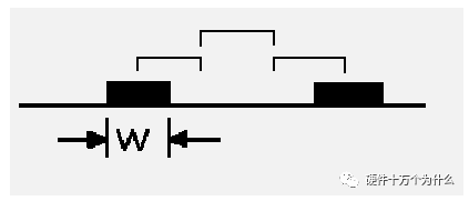
To reduce crosstalk between lines, ensure that the spacing between lines is sufficient. When the center-to-center spacing between lines is at least three times the line width, 70% of the electric field will not interfere with each other, known as the 3W rule. To achieve 98% of the electric field not interfering with each other, a spacing of 10W should be used.
(1) Clock, reset, signals above 100M, and some key bus signals must meet the 3W principle when routed with other signal lines. No long parallel lines should exist on the same layer or adjacent layers, and vias on the link should be minimized. (2) The number of vias for high-speed signals is a critical issue; some device manuals have strict requirements for the number of vias for high-speed signals. The principle of interconnection is that, apart from necessary fanout vias, no extra vias should be placed in the inner layers. They have routed 8G PCIe 3.0 with only four vias without issues. (3) The center distance of clock and high-speed signals on the same layer must strictly meet the 3H requirement (H being the distance from the routing layer to the return plane); signals on adjacent layers must not overlap, and it is recommended to also meet the 3H principle. Tools are available to check for the aforementioned crosstalk issues.
The main goal is to prevent mutual interference between modules operating at different frequencies while minimizing the routing length of high-frequency sections. For mixed circuits, it is also advisable to place analog and digital circuits on opposite sides of the printed board, using different layers for routing and isolating them with ground layers.
【1】Interest-driven passion
【2】Should hardware engineers design their own PCBs?
【3】How long should PCB traces be?
【4】How wide should PCB traces be?
【5】Inner layers of PCBs
【6】Vias
【7】Can PCBs have sharp angles and right angles?
【8】Should dead copper be retained? (PCB islands)
【9】Can vias be placed on pads?
【10】What material does FR4 refer to in PCBs?
【11】Why is the solder mask often green?
【12】Steel mesh
【13】Pre-layout
【14】Key points for PCB layout and routing
【15】Cross-segment routing
【16】Signal reflection
【17】Dirty signals
【18】Surface treatment processes such as gold plating, tin spraying, etc.
【19】Line spacing
【20】Placement of capacitors
【21】Crosstalk
【22】Flying probe testing of PCBs
【23】Overview and simulation of FPC
【24】Why do PCBs deform and bend? How to solve it?
【25】Understanding “characteristic impedance” in one article
【26】Layer design of PCBs
【27】Reflow paths for high-speed circuit PCBs
【28】Power handling and plane segmentation in PCB design
【29】Zigzag PCB routing – Tabbed routing
【30】What is the dielectric loss angle in PCBs?
【31】The impact of copper foil roughness on high-speed signals
【32】Why should crystal oscillators not be placed at the edge of PCBs?
【33】What are high-speed signals?
【34】What is a transmission line?
【35】Pre-emphasis, de-emphasis, and equalization
【36】How to utilize PCB heat dissipation
【37】”Stub” in PCB design
【38】Debate: Should there be a GND protection line between traces?
【39】PCB copper pouring
【40】Rules to follow when designing PCBs
【41】”Fake eight-layer” in multilayer PCB design
【42】In addition to strip lines and microstrip lines, there are also “co-planar waveguides”
【43】Parameters related to PCB pad design processes
【44】Why should grounding holes be drilled at the edges of PCBs?
【45】PCBs that are easier to dissipate heat: aluminum substrates
【46】Why should reference planes be hollowed out?
【47】PCB design for crystal oscillators
【48】Designing DC/DC power supply PCBs with EMC considerations
【49】PCB bends do not necessarily require arc routing to be the best
【50】Why should vias be blocked with “conductive via plug technology”?
【51】Key points for power PCB layout and routing
【52】Mark points on PCBs
【53】Simulating high-speed signal cross-segmentation with ADS
【54】Rigid-flex boards (soft-hard combined boards)
【55】Mixed digital and analog PCB design
【56】Placement of capacitors in PCB design
【57】The impact of via stubs in PCB design
【58】PCB design checklist: Structure
【59】PCB design checklist: Power
Hard Ten Published Books

“DCDC Power Supply” is currently in the publishing process, expected to be released in May, stay tuned.