Capacitors play a crucial role in high-speed PCB design and are typically the most used components on a PCB. In PCBs, capacitors are generally categorized into filtering capacitors, decoupling capacitors, and energy storage capacitors.
1. Power Output Capacitors, Filtering Capacitors
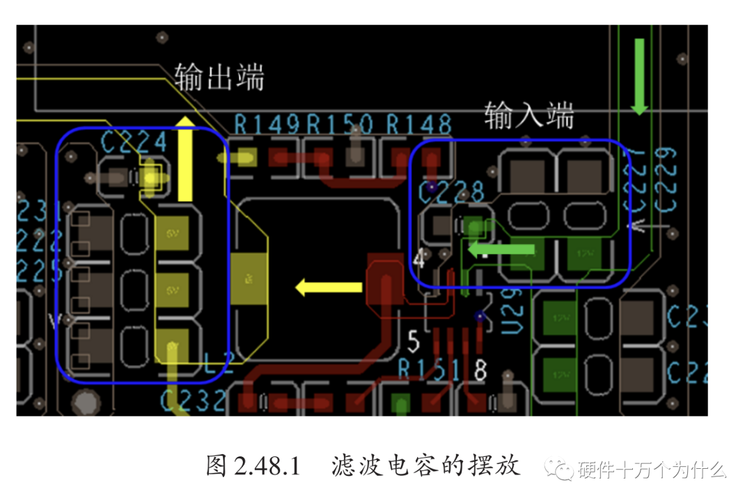
We usually refer to the capacitors in the input and output circuits of the power module as filtering capacitors. Simply put, they are capacitors that ensure the stability of the input and output power. In power modules, the principle for placing filtering capacitors is “larger first, smaller later.” As shown in Figure 2.48.1, the filtering capacitors are arranged in the direction of the arrow from larger to smaller.
During power design, it is important to ensure that the traces and copper areas are wide enough and that there are enough vias to meet the current carrying capacity requirements. The width and number of vias should be evaluated based on the current size.
Power Input Capacitors
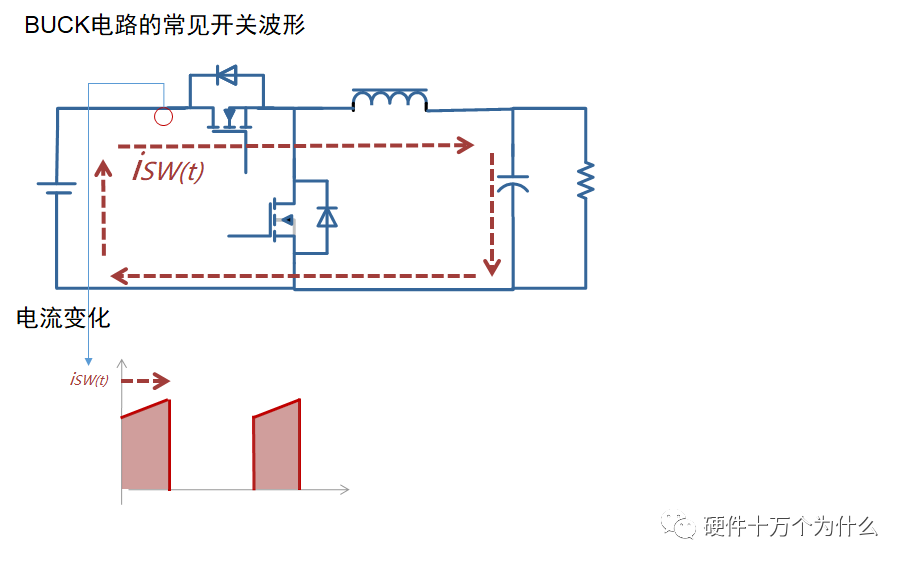
The power input capacitor forms a current loop with the switching loop. The variation in this current loop is significant, with the amplitude of Iout. The frequency corresponds to the switching frequency. During the switching process of the DC-DC chip, the current change generated by this current loop includes a rapid di/dt.
In synchronous BUCK configurations, the current path must pass through the chip’s GND pin, and the input capacitor should be connected between the chip’s GND and Vin, with the path as short and wide as possible.
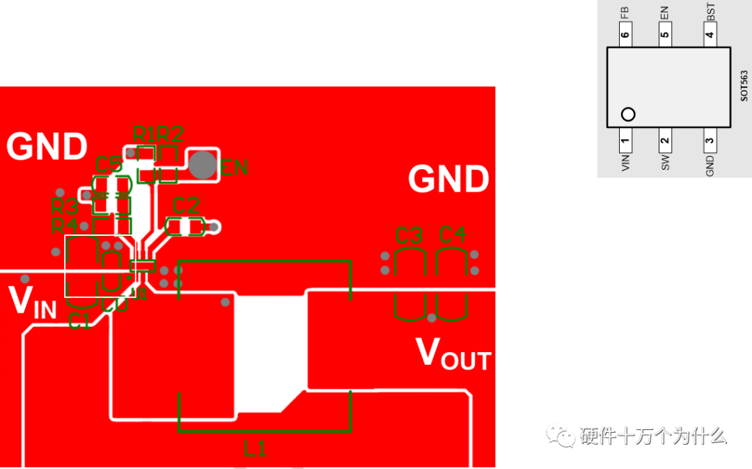
A smaller area for this current loop will improve its radiation performance.
2. Decoupling Capacitors
High-speed IC power pins require a sufficient number of decoupling capacitors, ideally one for each pin. In practical designs, if there is insufficient space for decoupling capacitors, they can be reduced as necessary.
The capacitance values for decoupling capacitors on IC power pins are usually small, such as 0.1μF or 0.01μF; the corresponding packages are also small, like 0402 or 0603. When placing decoupling capacitors, the following points should be noted:
(1) Place them as close to the power pins as possible; otherwise, they may not effectively decouple. Theoretically, capacitors have a certain decoupling radius, so the proximity principle should be strictly followed.
(2) The leads from the decoupling capacitors to the power pins should be as short as possible and should be thickened, typically with a width of 8 to 15 mils (1 mil = 0.0254 mm). The purpose of thickening is to reduce lead inductance and ensure power performance.
(3) After the leads from the decoupling capacitor’s power and ground pins exit the pads, they should be connected to the power and ground planes via nearby vias. These leads should also be thickened, and larger vias should be used whenever possible; for example, if a 10 mil via can be used, do not use an 8 mil via.
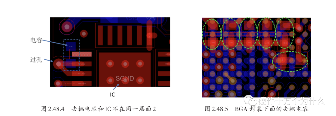
(4) Ensure that the decoupling loop is as small as possible. Common placement examples for decoupling capacitors are shown in Figures 2.48.2 to 2.48.4. The placement methods for SOP package IC decoupling capacitors are similar to those for QFP packages.
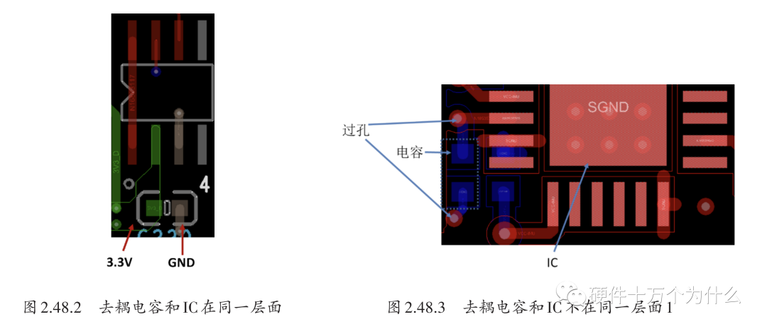
For common BGA packages, decoupling capacitors are usually placed underneath the BGA, on the back side. Due to the high pin density of BGA packages, the number of decoupling capacitors is generally limited, but as many as possible should be placed, as shown in Figure 2.48.5.
3. Energy Storage Capacitors
The role of energy storage capacitors is to ensure that the IC can provide electrical energy in the shortest time when in use. The capacitance values for energy storage capacitors are generally larger, and the corresponding packages are also larger. In PCBs, energy storage capacitors can be placed further away from the components, but not too far, as shown in Figure 2.48.6. Common fan-out methods for energy storage capacitors are shown in Figure 2.48.7.
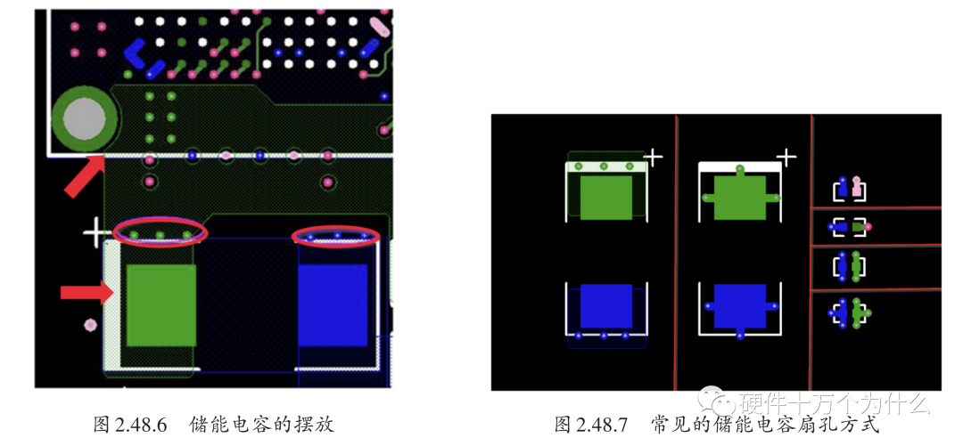
The principles for fan-out and fan-in of capacitors are as follows:
(1) Keep leads as short and thick as possible to minimize parasitic inductance.
(2) For energy storage capacitors or devices with high current, as many vias as possible should be used.
(3) Of course, the best electrical performance for fan-out is through-hole vias. Practical considerations must be taken into account.
This article is included in “The Hardware FAQ – Passive Components Edition”
For a comprehensive and systematic content on passive components (resistors, capacitors, inductors), you can purchase “The Hardware FAQ, Passive Components Edition”