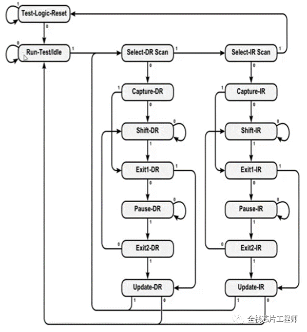
Question: JTAG has 5 ports, why is Trst an optional reset port?
Question: If JTAG only retains 4 ports, how do we reset without Trst?
Answer: The first question is simple; Trst can be replaced with Tms. What about the second question? Feel free to discuss in our knowledge community.
Question: After adding mbist and scan chain to the MCU chip design, what should we do if the simulation fails? First, diff the code to see what changes were made and if they were done correctly. Then perform 2-3 formal/lec checks to ensure the DFT implementation process does not alter the functionality. Additionally, ensure that the DFT port control signals at the top level are correctly instantiated in the testbench, such as ensuring the JTAG port can be used for CPU debugging and mbist testing, and pay attention to TDO output selection control.
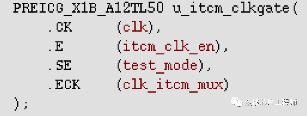
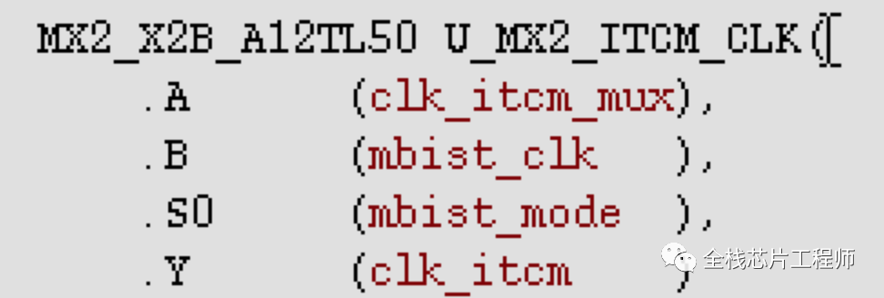
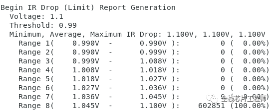
Back to the main topic, after DFT insertion, a large number of multiplexers are added to control the clock and reset, resulting in cells in the intermediate net labeled with delay parameters specified by the process library file, which defaults to 1ns. This can cause clock delays; for example, inserting two levels of multiplexers can create a 2ns delay. Our MCU runs at 250MHz, with a clock cycle of 4ns, and if the SRAM clock is inverted, it can easily cause SRAM timing issues, leading to SRAM outputting ‘x’ state and the CPU failing to fetch instructions.
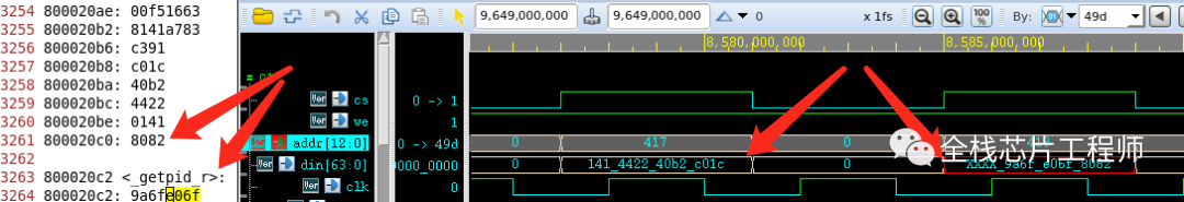
As shown, control signals like cs/we for SRAM are aligned with the SRAM clock, causing the SRAM model to output ‘x’ state, leading to CPU instruction fetch failure and MCU boot failure.
Students in the Jingxin SoC training camp know, or are familiar with DFT simulation, that VCS simulation should add an option; if you don’t know, hurry to find me!
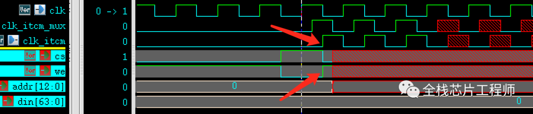
You can forcibly clock the system by selecting a clock that can sample cs/we and other SRAM control signals. Unfortunately, the CPU executed part of the instructions and then stopped, continue debugging.
Check whether the RISC-V assembly instructions read and write correctly:
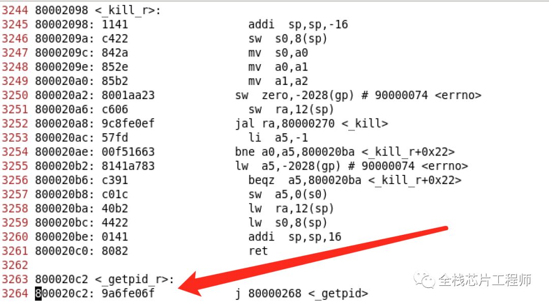
At the end of the program, there is an ‘x’ state. Students will ask why there is an ‘x’ state in the instructions; it must be due to a bug or timing issue. Let’s take a look:
The ‘x’ state above is due to the CPU having 16-bit instructions and the program having jumps. So why did the CPU stop executing after part of the instructions? Did I modify the instruction fetch module incorrectly? Then I started to look at the CPU code…
In fact, the program can still execute correctly after the ‘x’ state; the essence is due to the 16-bit instruction and program jumps. Next, debug.

Next, locate the issue; it turns out to be the instruction fetch handshake is stuck. What is the solution? How to ensure clock alignment in post-simulation? Refer to the full-stack chip engineer’s knowledge community.
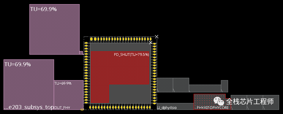
Challenge! Full chip UPF low power design (including DFT design)
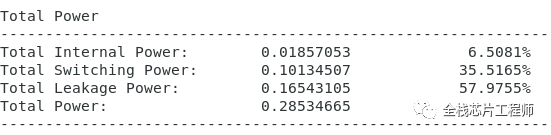
The Jingxin SoC training camp project reports a power consumption of 27.9mW before low power design.

After low power design, the power consumption is 0.285mW, a reduction of 98.9%!
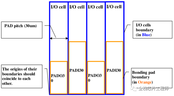
In the 7-day sprint PR training camp, students asked how to add PAD to IO? Please think about how to achieve the best implementation of Jingxin SoC’s IO and PAD?
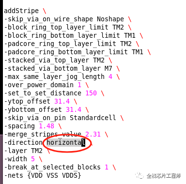
In the 7-day sprint PR training camp, some students asked, with the same floorplan, why some students finished quickly while others encountered numerous DRC issues (EDA tools repeatedly iterating) causing the tools to never finish. What specific issues are there?
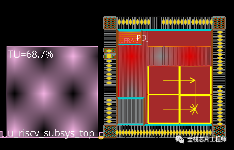
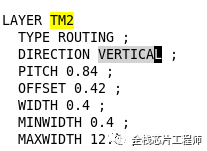
First, I found that the student’s stripe defined TM2 as horizontal, while those familiar with Jingxin’s process know that TM2’s preference direction is VERTICAL.
Querying Jingxin’s LEF library file can also confirm:
How significant is the impact of using the wrong direction? Everyone should practice on Jingxin SoC’s backend flow to gain true knowledge.
In the 7-day sprint PR training camp, a student asked why the PR took a day and night (24 hours) to complete routing but still had numerous DRC errors? I have minimized the design scale to speed up PR design; in fact, routing can be completed in 2 hours, so why is it so slow? The reason is the routing of low-power cells. For specific reasons and solutions, feel free to join the Jingxin training camp for discussion.
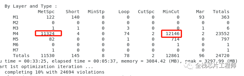
The errors are mainly concentrated on M4; please think about how to solve it.
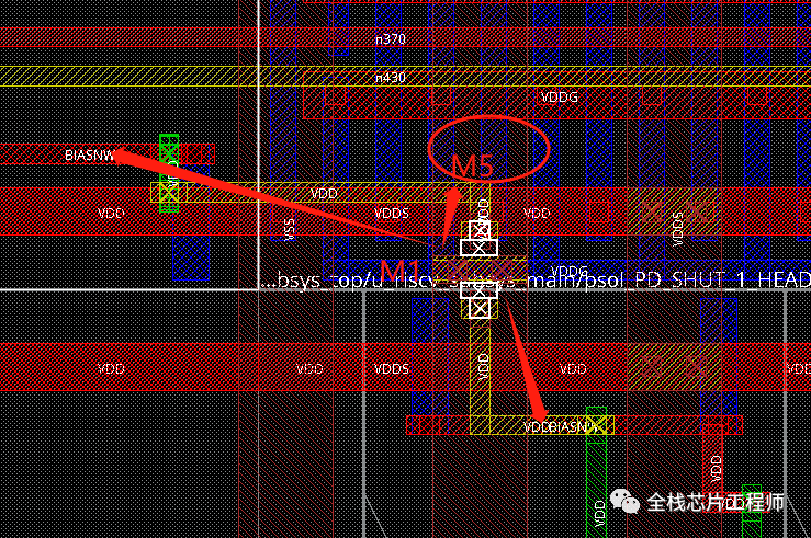
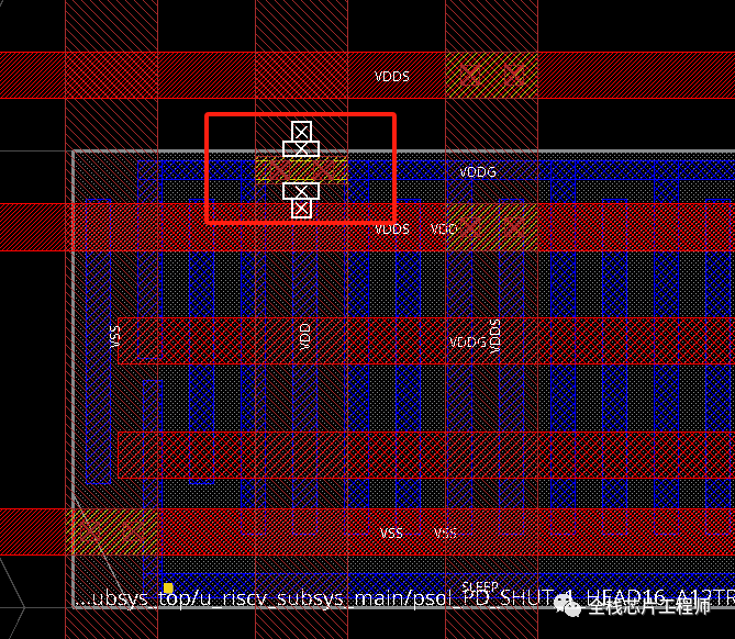
In the 7-day sprint PR training camp, a student asked why the second PG pin (VDDG) of the power switch cell is connected from M1 instead of M2. Please think about what issues this may cause and how to resolve it.
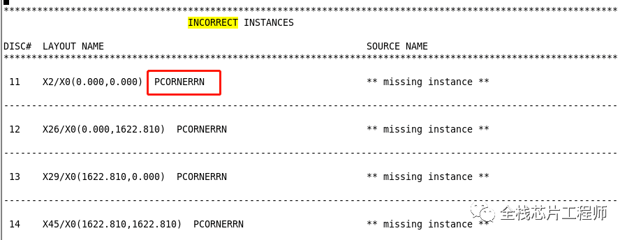
In the 7-day sprint PR training camp, a student asked how to handle LVS failures at Corner Pad encountered by students in the Jingxin SoC training camp.
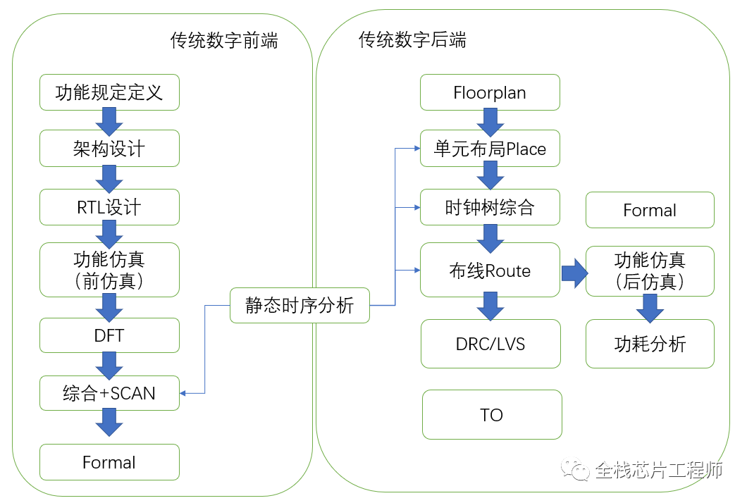
After completing the front-end design simulation and DFT of the Jingxin SoC training, we move to the backend flow. This tutorial teaches you how to complete the digital backend flow with one click.
The script command to generate is as follows:
tclsh ./SCRIPTS/gen_flow.tcl -m flat all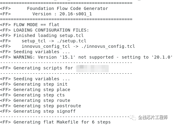
Before generating the flow script, setup.tcl and other related parameters need to be configured. For details, refer to the unique all-stack chip engineer’s self-developed Jingxin SoC front-end engineering, DFT engineering, and backend engineering, guiding you through the entire SoC project design process from algorithms, front-end, DFT to backend.
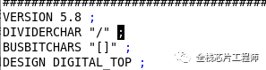
Students in the Jingxin SoC training camp asked why Innovus reports an error when reading the completed floorplan DEF file? First, check the log:
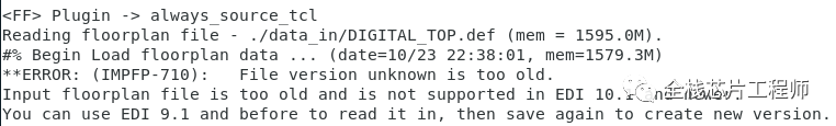
Reading floorplan file – ./data_in/DIGITAL_TOP.def (mem = 1595.0M).
#% Begin Load floorplan data … (date=10/23 22:38:01, mem=1579.3M)
**ERROR: (IMPFP-710): File version unknown is too old.
In the past EDI period, we could load the floorplan by defining fp_file:
set vars(fp_file) "./data_in/DIGITAL_TOP.def"However, now Innovus has upgraded and abandoned the fp_file loading method. Of course, you can use the old version of EDI 9.1 and earlier to add fp_file and then save it as a new version, but this method is obviously unnecessary. As the log prompts, checking the log is a very good engineering habit.
Input floorplan file is too old and is not supported in EDI 10.1 and newer.
You can use EDI 9.1 and before to read it in, then save again to create a new version.
My intuition tells me to check which DEF version the student saved the file in?
The student’s saving method is as follows:
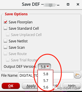
So how do we solve this? Please join the Jingxin training camp to practice.
The Jingxin SoC used many asynchronous FIFOs; students interested in the asynchronous RTL implementation can extract the asynchronous FIFO to view the layout connections:
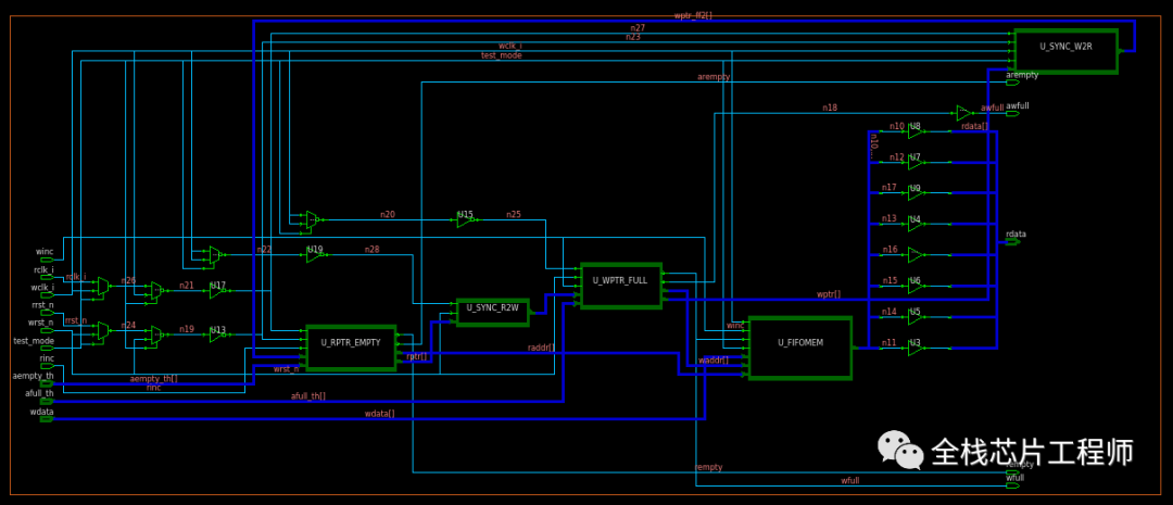
Check the area of all asynchronous FIFO cells;
dbget [dbget top.insts.pstatus unplaced -p].areaCheck the names of all asynchronous FIFO cells:
dbget [dbget top.insts.pstatus unplaced -p].nameSo how do we extract asynchronous paths to observe the layout routing? How to report timing? For more content, refer to the knowledge community and SoC training camp.