Does IIC support hot swapping? (With a detailed interpretation of CW32 IIC protocol) Have you learned it yet? After I finish these low-speed experiments, I will provide the debugging steps for the logic analyzer.
IIC is done, next comes SPI, which is worth highlighting because the vast majority of devices use SPI; it’s practically ALL IN.
I believe everyone shouldn’t be too troubled by protocols; they are designed by humans, and if you grasp the core concepts, you can extrapolate. For example, how data is transmitted as 0s and 1s within a protocol. Yes, it’s that simple. Also, knowing the size of each transmission frame is crucial; if it’s smaller, pad it with 0s, and if it’s larger, split it into multiple frames.
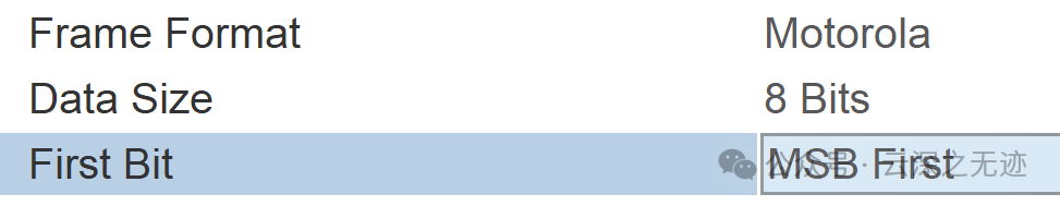
Data transmission in SPI is framed, and the data width per frame is typically 8 bits (can also be configured to 16 bits or more). Data can be sent starting from MSB (Most Significant Bit) or LSB (Least Significant Bit), depending on device configuration.
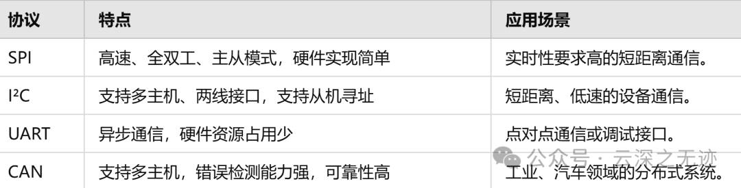
In fact, the characteristics of SPI are freedom, simplicity, and high speed.
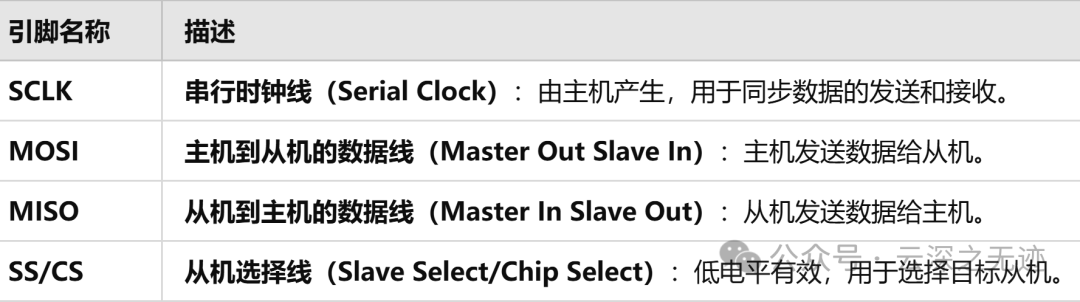
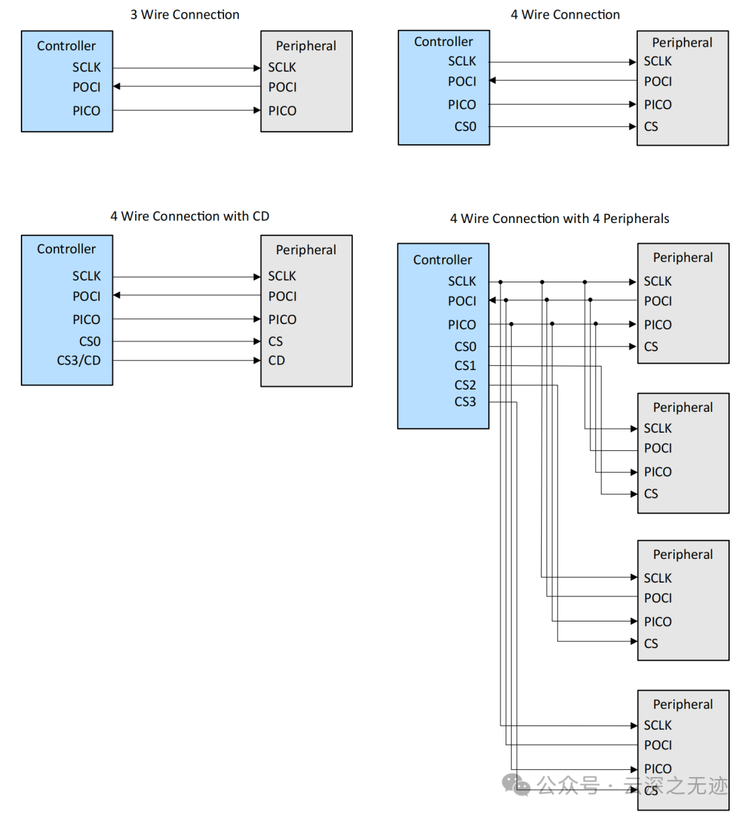
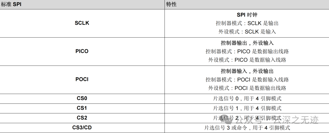
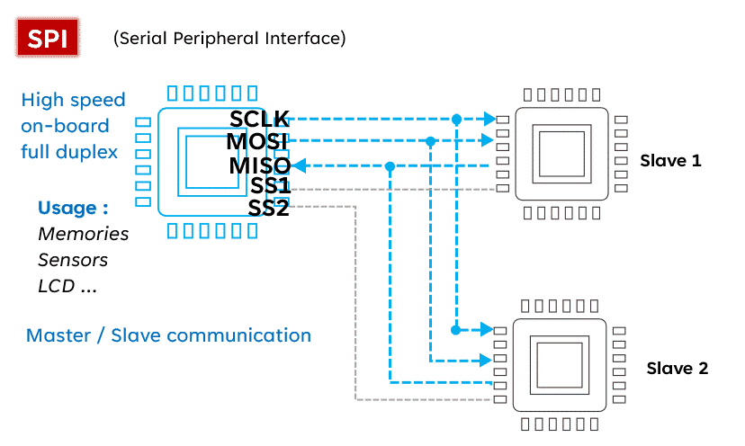
The pin standard is 4 pins, with many variants.
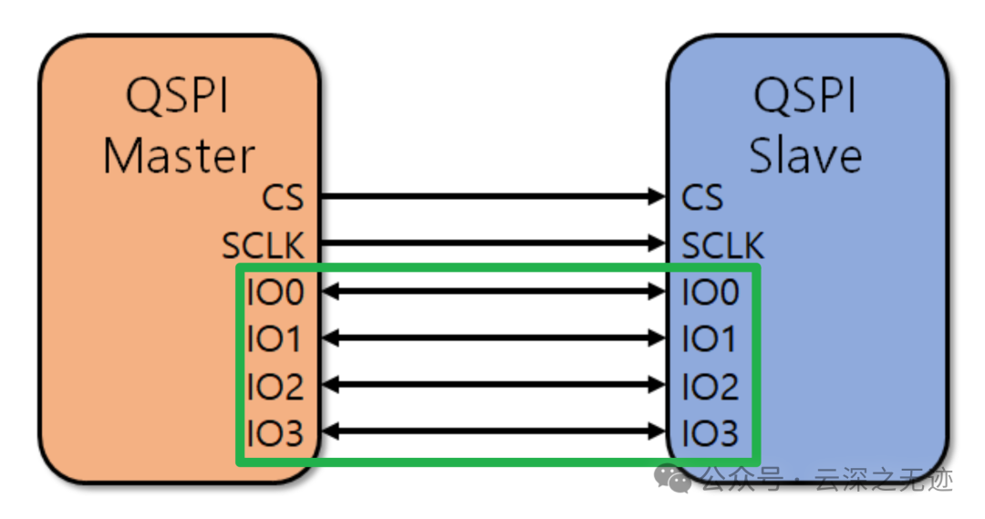
For instance, QSPI uses 4 data lines together to output, with 4 bits per clock edge.
SPI synchronizes data transmission through the clock signal (SCLK).
First, observe SCLK, then check where the stable sampling occurs.
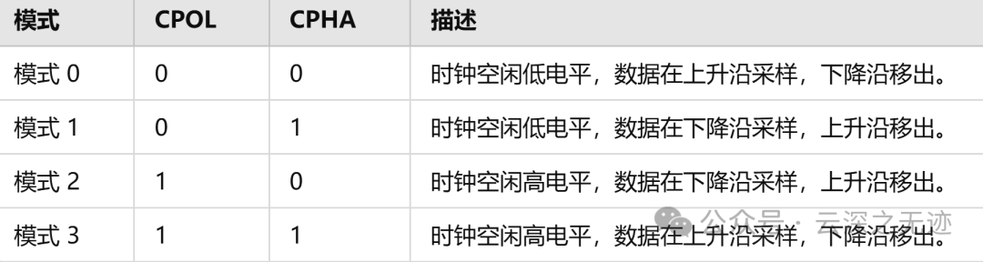
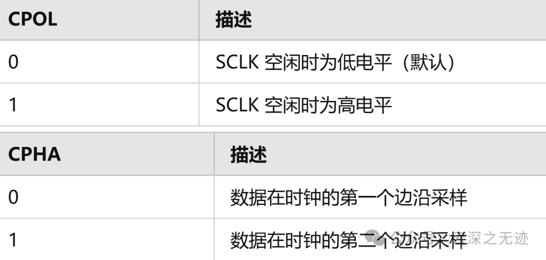
There are four combinations.
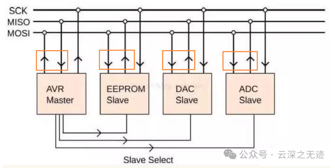
Single Master Communication
-
The master pulls the target slave’s SS/CS pin low (active), while other slaves remain inactive.
-
After communication is complete, the master pulls the SS/CS pin high (inactive).
Multi-Slave Communication
-
Each slave is assigned a separate SS/CS pin.
-
The master selects the target slave by controlling the corresponding SS/CS pin.
-
Multiple SPI devices’ SCK, DIN, DOUT can be connected to peripheral ports, with CS connected separately; once pulled low, the master knows this device is to communicate.
Next, we will look at a more straightforward interpretation.
-
First interaction: The customer says to the chef, “I want a hamburger.” The chef cannot provide the hamburger immediately but will chat (send meaningless data). -
Second interaction: The customer asks, “Is my hamburger ready?” (Dummy Data), and at this point, the chef has prepared the hamburger and hands it to the customer (returns valid data).
This color illustrates the situation well; gray indicates that data is being sent.
The core of SPI communication is synchronous sending.

Synchronous
Next, let’s look at how SPI is implemented in different MCUs:
NRF5280, so you also refer to IIC as TWI.
It can be seen that SPI is preferred over IIC for its freedom and efficiency.
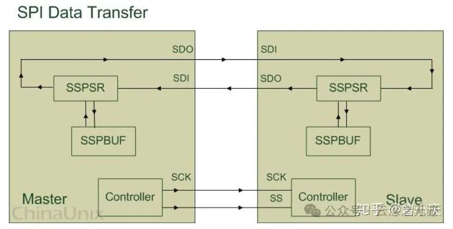
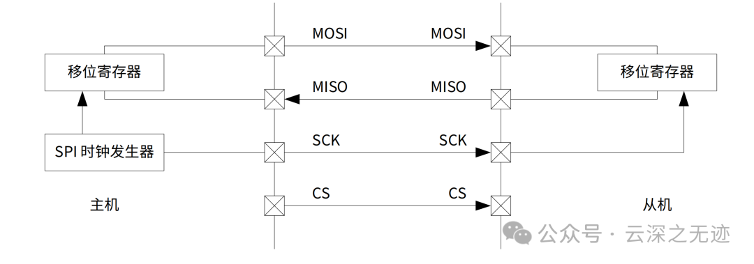
During SPI communication, data sending (serially shifted out to the MOSI/SDO bus) and receiving (sampling or reading data on the bus (MISO/SDI)) occur simultaneously. The serial clock edge synchronizes the shifting and sampling of data.
On each clock edge, the two pins exchange once.
During each Clock cycle, the SPI device sends and receives a bit of data (regardless of whether it is the master or slave), meaning that a bit of data is exchanged by the device.
Assuming the master sends data 0b1010, the slave will simultaneously return data 0b0101.
This diagram illustrates the cyclic process well.
MicroChip’s peripherals
Rotating exchange
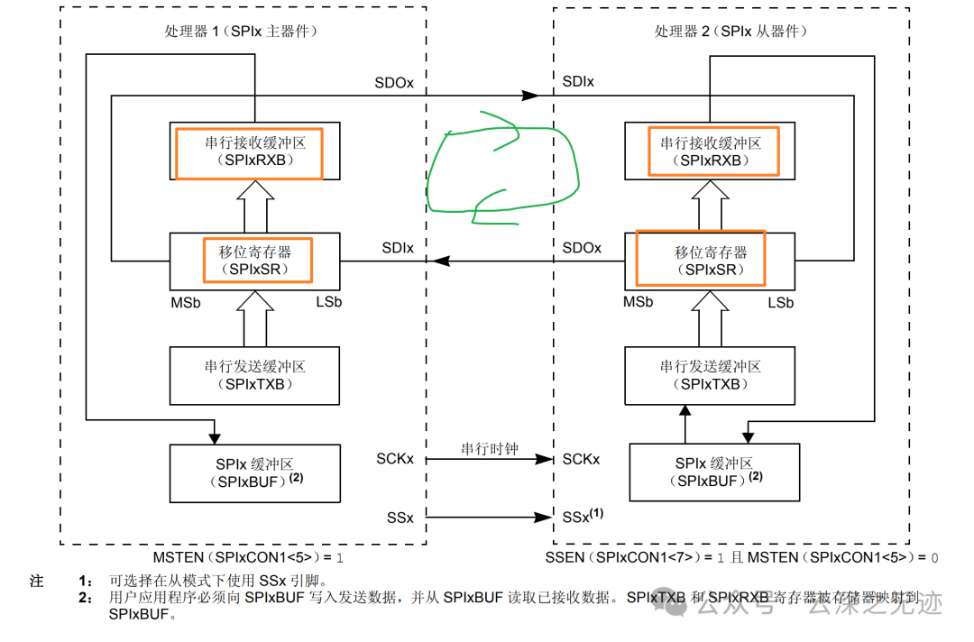
For a Slave device to receive control signals from the Master, it must first be accessible by the Master.
Thus, the Master must first select the Slave device through the SS/CS pin to enable communication.
During data transmission, each received piece of data must be sampled before the next data transmission. If the previously received data is not read, it may be discarded, leading to the eventual failure of the SPI physical module.
-
Each SPI peripheral (whether master or slave) has send and receive registers. -
When each SPI clock cycle is completed, the received data is stored in the receive register, while the data in the send register is sent out.
Therefore, in programs, it is common to read data from the SPI device after data transmission, even if this data (Dummy Data) is useless in our program (although reading immediately after sending is meaningless, it still needs to be read from the register).
After each data reception, the program must read data from the receive register; otherwise, new data arriving will overwrite the original data (data loss).
This is why even if the program does not care about certain data (such as dummy data), it must be read out through code.
-
Write operations will simultaneously receive Dummy data:
-
Read operations require sending Dummy data:
When the master sends data to the slave, the slave’s MISO pin will also output data (which may be meaningless Dummy data, such as 0xFF or 0x00).
If the master only wants to “write data,” it needs to ignore the received data.
When the master needs to read data from the slave, it must send some meaningless placeholder data (Dummy data, such as 0xFF or 0x00) via MOSI to trigger the clock signal to drive the slave’s data transmission.
Only then can the master obtain valid data from the slave’s receive register.
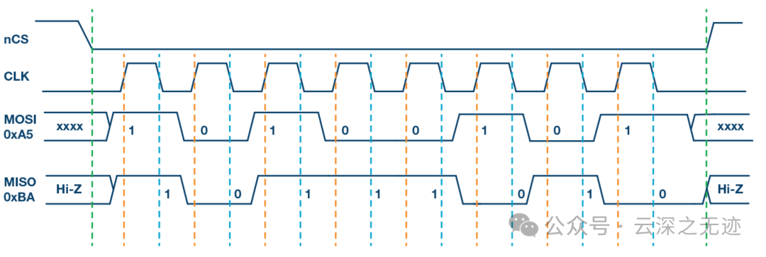
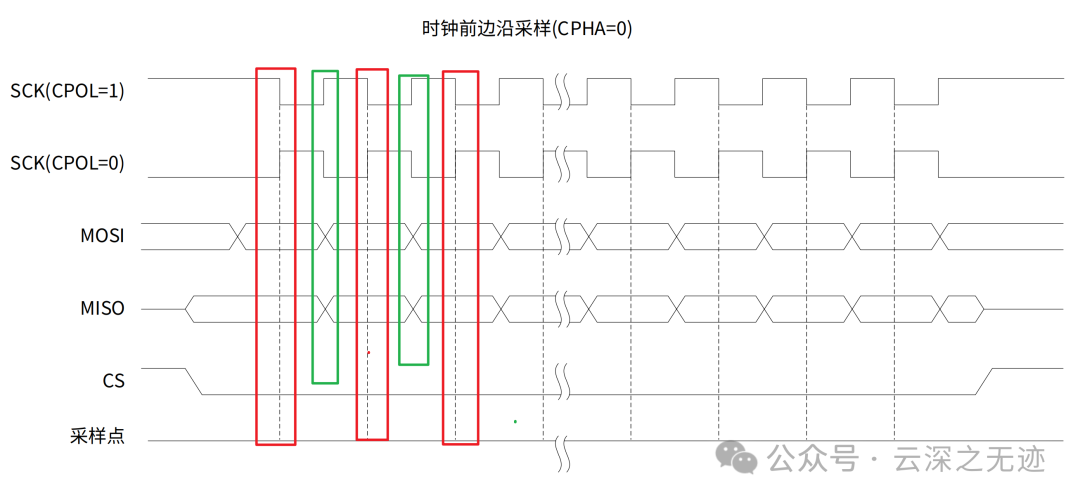
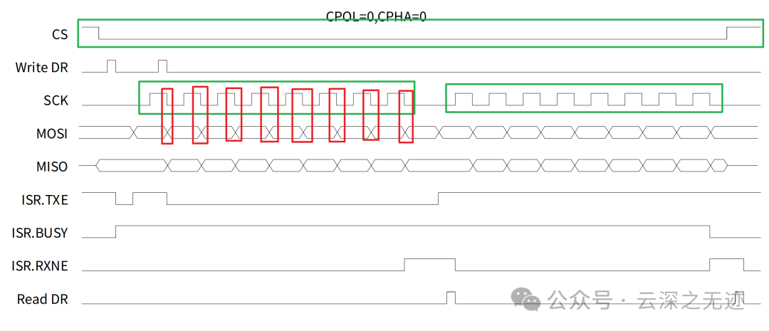
CLK idle state = low level, data is sampled on the rising edge and shifted out on the falling edge.
Data is displayed on the MOSI and MISO lines. One sends and one receives.
The start and end of transmission are indicated by green dashed lines, the sampling edge by orange dashed lines, and the shifting edge by blue dashed lines.
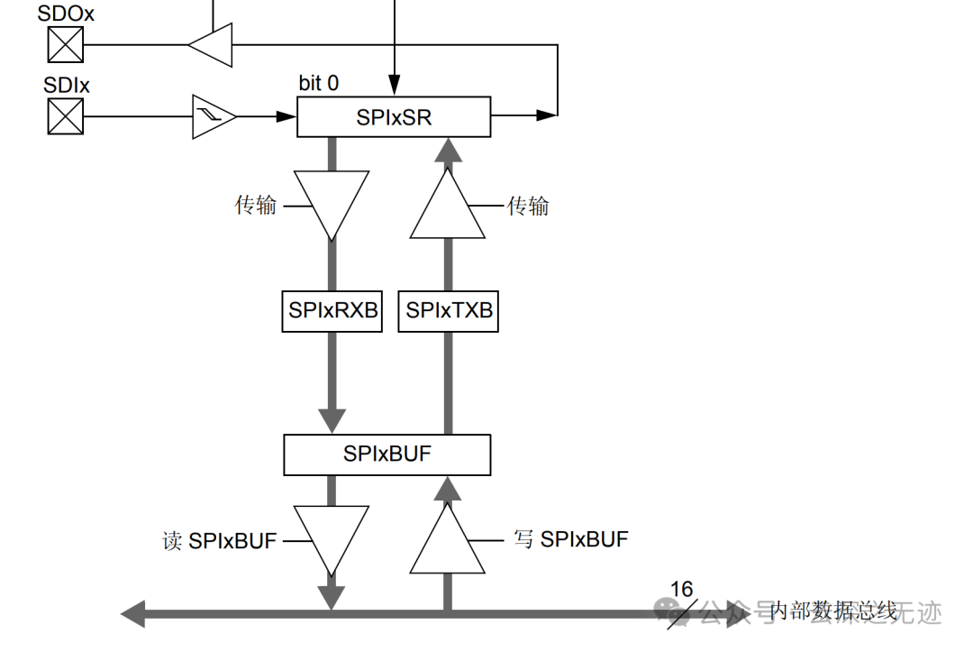
In SPI communication, “shifting out” refers to data being transmitted from the send register to the MOSI (Master Output Slave Input) pin or MISO (Master Input Slave Output) pin, ultimately received by the other device.
Let’s look at the transmission process from the edge perspective.
-
The sampling edge of one device corresponds to the shifting edge of another device. -
For example: if sampling occurs on the rising edge of the clock, data is usually shifted out on the falling edge.
Now let’s look at each component:
-
Inside the SPI device:
-
The SPI register stores the data to be sent.
-
On the falling edge of the clock, the data in the register is shifted out to the hardware transmission logic and output to the pins (MOSI or MISO).
SPI bus:
-
Data is transmitted on the bus (MOSI or MISO line), sent to the other device with the change of the clock signal.
-
Simultaneously, the other device will sample and receive that data based on the rising edge of the clock.
The other device:
-
The receiving party samples the data on the bus at the clock’s rising edge, storing the received data signal in its own receive register.
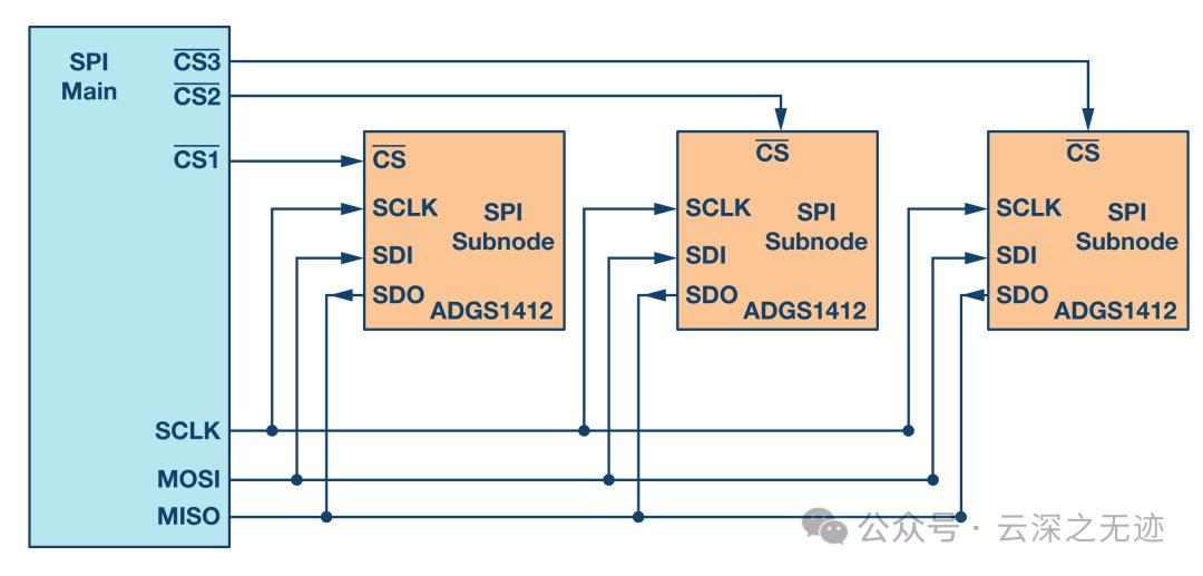
Multiple devices can be connected.
There are many connection methods – MSPM0 diagram.
TI has taken a new name; it’s written in a relatively straightforward manner.
TI’s data sheet is quite difficult to read, not user-friendly.
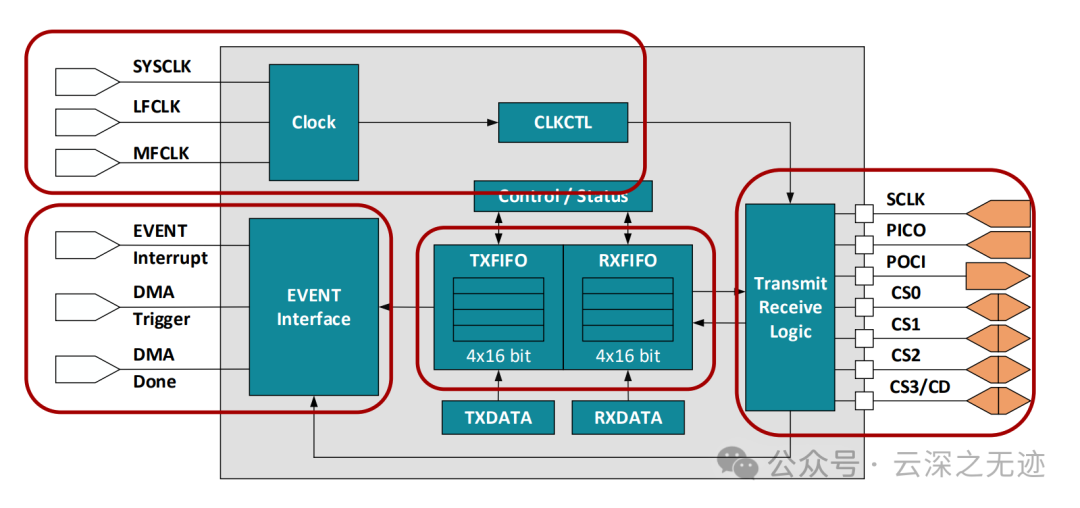
As usual, we start with the CW32 reference manual.
The Serial Peripheral Interface (SPI) is a synchronous serial data communication interface commonly used for synchronous serial communication between MCUs and external devices.
The CW32L010 integrates one serial peripheral SPI interface, supporting bidirectional full-duplex, single-line half-duplex, and simplex communication modes, configurable as either master or slave, and supports multi-master communication mode.
-
Fast speed: SPI communication can reach tens of Mbps, making it more efficient than I²C. -
Full-duplex: Supports simultaneous sending and receiving of data. -
Simple protocol: No complex handshakes or addressing mechanisms.
This is a feature function.
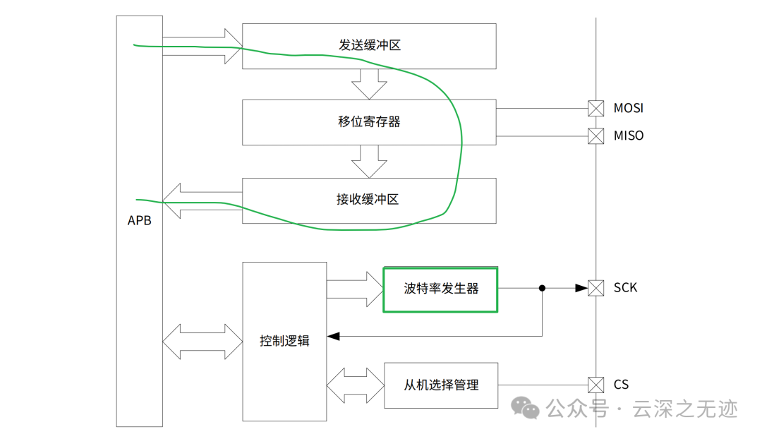
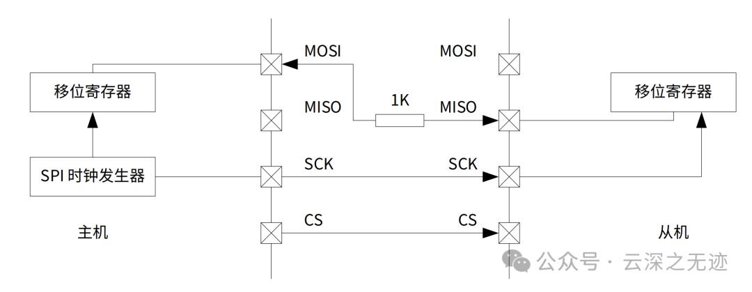
This block diagram is very simple, just sending and shifting forming a loop, plus a clock and CS.
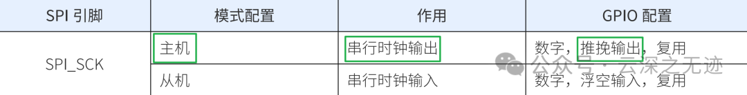
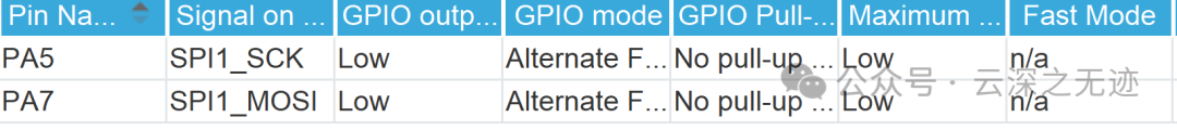
First, look at GPIO; the clock is an output, and it still needs driving capability, push-pull.
Very comprehensive; CH’s data sheet has this too.
The communication timing of SPI, CS, SCK, and MOSI signals are all controlled and generated by the master, while the MISO signal is the slave’s response signal.
Slave selection CS signal transitions from high to low, marking the start of SPI communication. When the slave detects the start signal, it begins communication with the master.
During each SCK clock cycle, the MOSI and MISO signal lines transmit one bit of data. CS transitions from low to high, signaling the end of communication, indicating that the current communication has concluded.
Do you think this statement is unremarkable?
I’ll quiz you: Is the clock always present? Or is it only available during communication?
Clearly, the master provides the clock, synchronizing the outgoing data.

You can continue to zoom in.
-
Generated by the master and provided to the slave. -
Used to synchronize data transmission between master and slave. -
The sampling moment of the data is determined by the clock signal’s edge (rising or falling). -
The slave passively receives the clock signal and cannot actively generate the clock.
-
The clock signal (SCK) is activated by the master at the start of communication and stops when communication ends. -
In non-communication states, SCK remains at the idle level (determined by clock polarity CPOL).
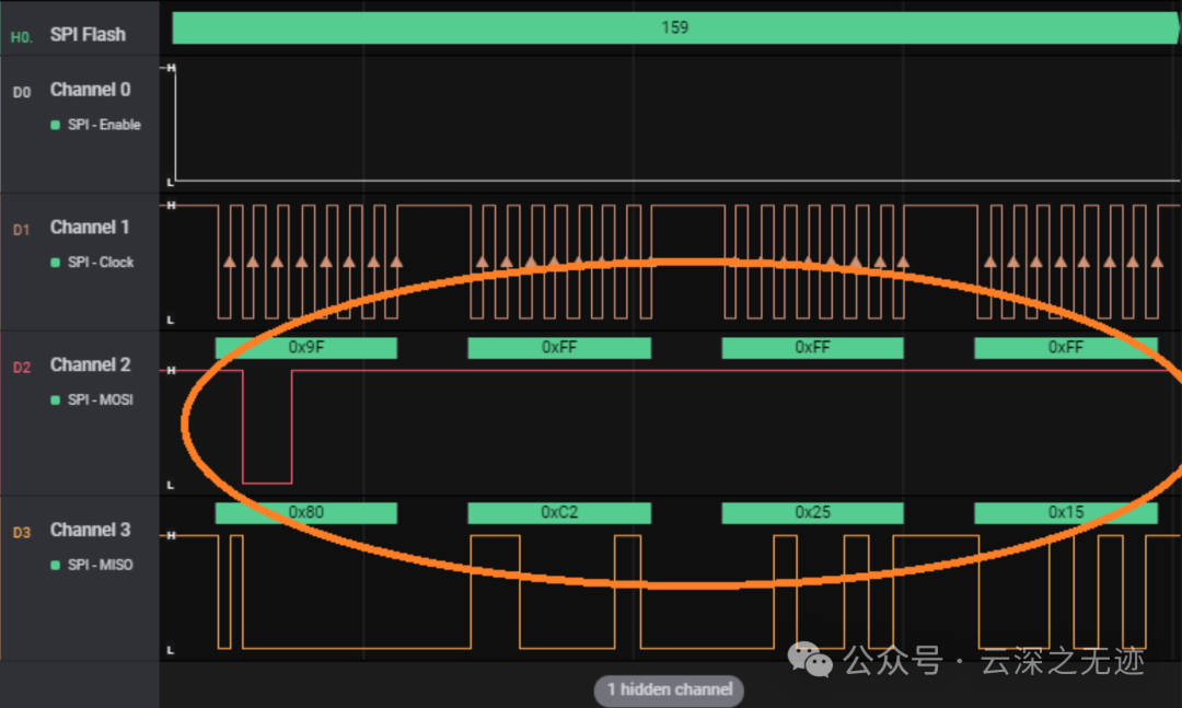
The falling edge is a sampling point; the data line is stable, capturing 0 or 1. On the next edge, the red indicates a data change.
Data lines crossing indicates changes, and values cannot be taken as they are unstable.
The data frame width is configured by the control register SPI_CR1’s WIDTH field, allowing for a data width of 4 to 16 bits.
We will look at the register specifics later; it indicates how many bits a data frame contains; we typically use one byte, 8 bits.
STM32 specifies 16 bits and 8 bits, not that flexible.
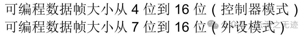
MSP allows arbitrary encoding.
The endianness of data is configured by the control register SPI_CR1’s LSBF field, allowing for the selection of the most significant bit first (MSB) or least significant bit first (LSB).
The master mode frame interval is configured by the control register SPI_CR1’s GAP field, allowing for the selection of 0 to 15 SCK clock cycles.
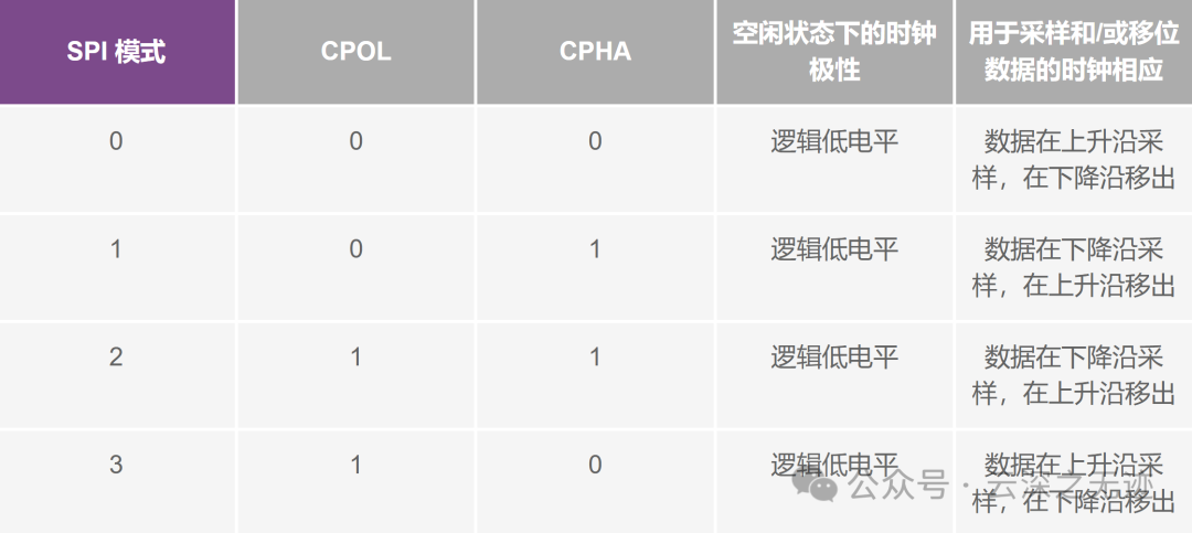
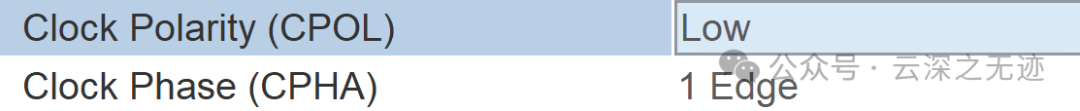
Clock polarity CPOL indicates the level state of the SCK serial clock line when the device is in an idle state without data transmission.
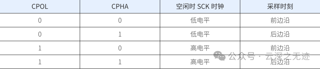
There are four types.
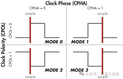
First, observe the clock; if it is 0, the first edge during operation is rising, and sampling can occur at this time or on the next edge, which is falling. It’s very simple; always remember the stable sampling time.
ADI’s diagrams are very nice.
I like ST’s design; it’s very intuitive.
Full-Duplex Mode:
The master sends data via MOSI while simultaneously receiving data via MISO.
Data is exchanged in bits simultaneously; for example, while the master sends a byte, the slave also returns a byte.
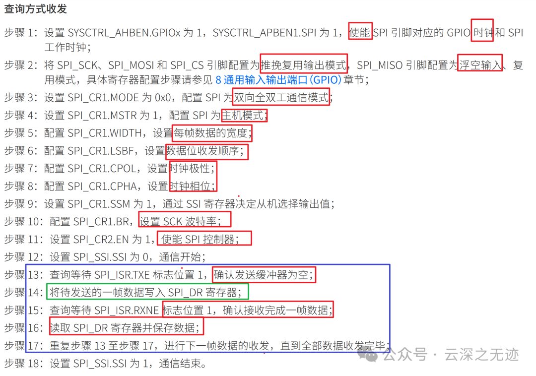
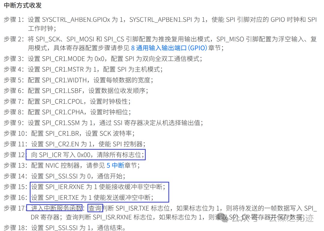
Set SPI_CR1.MSTR to 1 for the SPI to operate in master mode. Actively send clock signals.
Set SPI_SSI.SSI to 0, with the master selecting the CS pin to output low as the start signal. The initial flag is that CS is pulled low; all units take note.
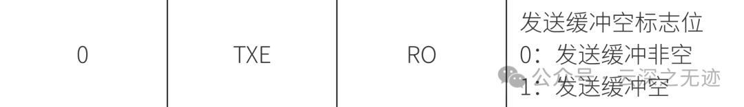
When the send buffer is empty, indicated by SPI_ISR.TXE being 1, write a frame of data to the SPI_DR register. Under the control of the synchronous shifting clock signal, data is output from the MOSI pin while the data from the MISO pin is received into the shift register.
The master sends nothing at this point; this state flag is 1. At this time, the data to be sent needs to be written in, followed by transmission under clock synchronization. Simultaneously, the receiving buffer retrieves data from the slave.
When the sending of a data frame ends, the receive buffer not empty flag SPI_ISR.RXNE is set to 1 by hardware, indicating that a frame of data has been received. At this point, the SPI_DR register can be read.
Set SPI_SSI.SSI to 1, with the slave select pin CS outputting high, indicating the end of this communication.
The pin is pulled low, and a frame is completed.
How do we ensure the integrity of a data frame during sending?
First, the CS pin indicates the synchronization flag.
Second, the sampling edge on the clock pin.
CS and SCK are two important signals.
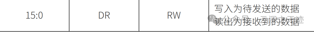
DR is the data written; it’s just preparation, aren’t you sending?
Prepare the contents of this register before MOSI.
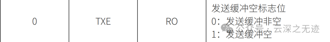
This indicates whether the buffer has content.
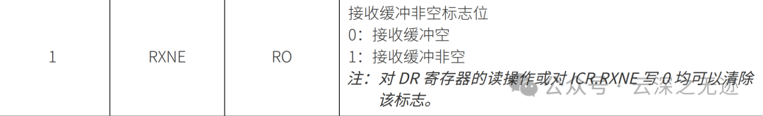
Similarly, the receiving buffer can also have a status; good stuff.
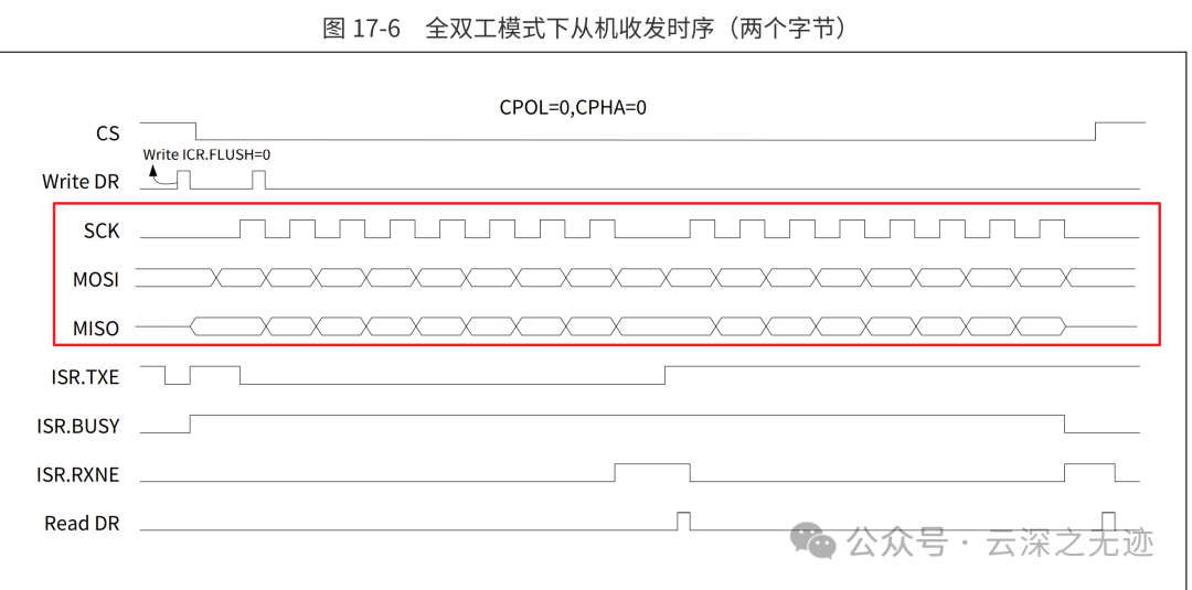
Now let’s look at slave transmission and reception.
Set SPI_CR1.MSTR to 0 for SPI to operate in slave mode.
Before the CS signal is pulled low, the slave needs to set SPI_ICR.FLUSH to 0 to clear the send buffer and shift register, writing the first frame of data to the SPI_DR register.
When the CS signal is pulled low, the data written will be output from the MISO pin under the control of the master’s synchronous shifting clock signal while receiving data from the MOSI pin into the shift register.
If it is multi-frame continuous communication, the user should continuously check the SPI_ISR.TXE flag; once the flag is 1, immediately write the data to be sent into the SPI_DR register to avoid data loss.
Once it is empty, write the data in. The buffer’s role is to determine when it is empty before sending.
When the receive buffer is not empty, indicated by SPI_ISR.RXNE being 1, it means a frame of data has been received. At this point, the SPI_DR register can be read. When the CS pin transitions to high, this communication ends.
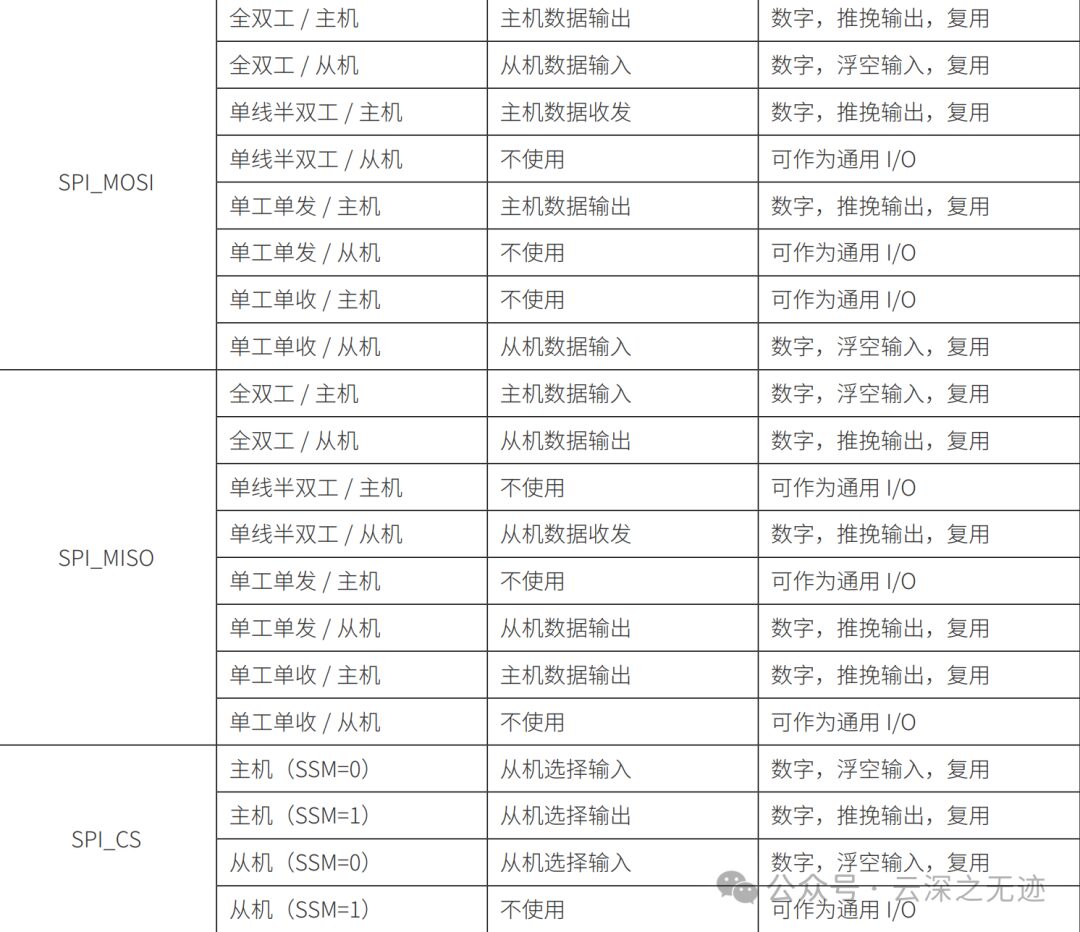
It can be seen that there is only one line, bidirectional.
In single-line half-duplex communication, due to the inability to guarantee synchronous switching of communication direction between the master and slave, driving conflicts may occur, potentially damaging the devices. It is recommended to connect a resistor in series on the data line between the master and slave to limit current.
When SPI operates as a slave, using single-line half-duplex mode allows for synchronous communication with a standard UART transceiver. In this case, SPI must be configured to fixed level mode: clock polarity CPOL is 1, clock phase CPHA is 1.
The master sends
Set SPI_CR1.MSTR to 1 for SPI to operate in master mode; set SPI_CR3.HDOE to 1 for the master to send data only.

1 indicates sending only.
The master sets SPI_SSI.SSI to 0, with the slave select pin CS outputting low as the communication start signal.

These are the start signals, quite complex.
When the send buffer is empty, indicated by SPI_ISR.TXE being 1, write a frame of data to the SPI_DR register, with data output from the MOSI pin under the control of the synchronous shifting clock signal.
After writing the last frame of data, wait for the send buffer to be empty, indicated by SPI_ISR.TXE becoming 1, and SPI_ISR.BUSY becoming 0, to ensure that data has been fully sent.
Then set SPI_SSI.SSI to 1, with the slave select pin CS outputting high, ending this communication.
It’s dull…
Next, let’s look at an STM32C0 chip:

Two lines suffice.
Two lines are enough for communication.

It can be seen that ST has DMA support across its entire series.
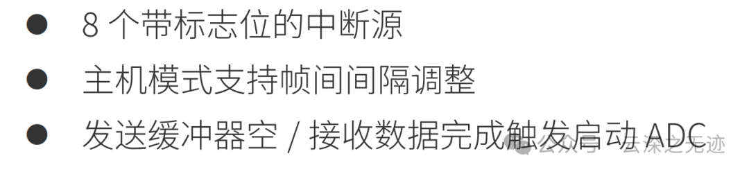
The SPI controller supports 8 interrupt sources. When a SPI interrupt-triggering event occurs, the interrupt flag will be set by hardware. If the corresponding interrupt enable control bit is set, an interrupt request will be generated.
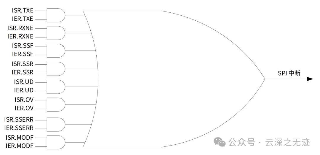
Yay, interrupts are here.

Once interrupts are enabled, it’s a big interrupt; the specifics of which interrupt depend on the register information.
In the user SPI interrupt service routine, relevant SPI interrupt flags should be checked for appropriate handling, and before exiting the interrupt service routine, the interrupt flag must be cleared to avoid re-entering the interrupt routine.
Very simple to use.
The old rule is to read status and write data.
Interrupt mode is a bit more complex because it requires clearing and handling the buffer.
Let’s take a look at STM32’s.
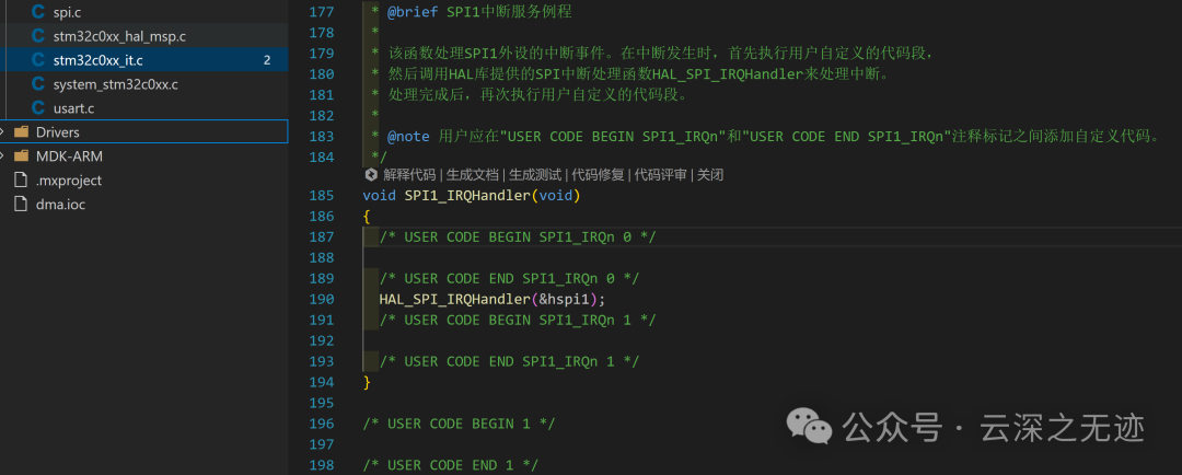
Interrupts are here.
It’s necessary to determine which interrupt occurred.
Then write a callback function.
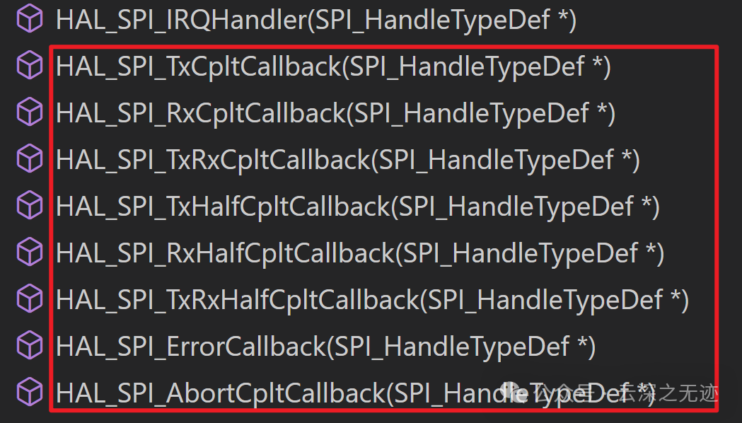
If it is a full duplex completion:
void HAL_SPI_TxRxCpltCallback(SPI_HandleTypeDef *hspi){ if (hspi->Instance == SPI1) // Ensure it is SPI1 { // Handle the received data (rx_buffer contains received data) for (int i = 0; i < sizeof(rx_buffer); i++) { printf("Received Data[%d]: 0x%02X\n", i, rx_buffer[i]); } // Here you can continue to the next communication if needed }}To send data only:
void HAL_SPI_TxCpltCallback(SPI_HandleTypeDef *hspi){ if (hspi->Instance == SPI1) { printf("SPI Transmit Completed!\n"); }}But it needs to be in NVIC:
void HAL_MspInit(void){ HAL_NVIC_SetPriorityGrouping(NVIC_PRIORITYGROUP_4); // Configure the interrupt priority for SPI1 HAL_NVIC_SetPriority(SPI1_IRQn, 0, 0); HAL_NVIC_EnableIRQ(SPI1_IRQn);}That’s all.
However, TI’s microcontrollers are more interesting:
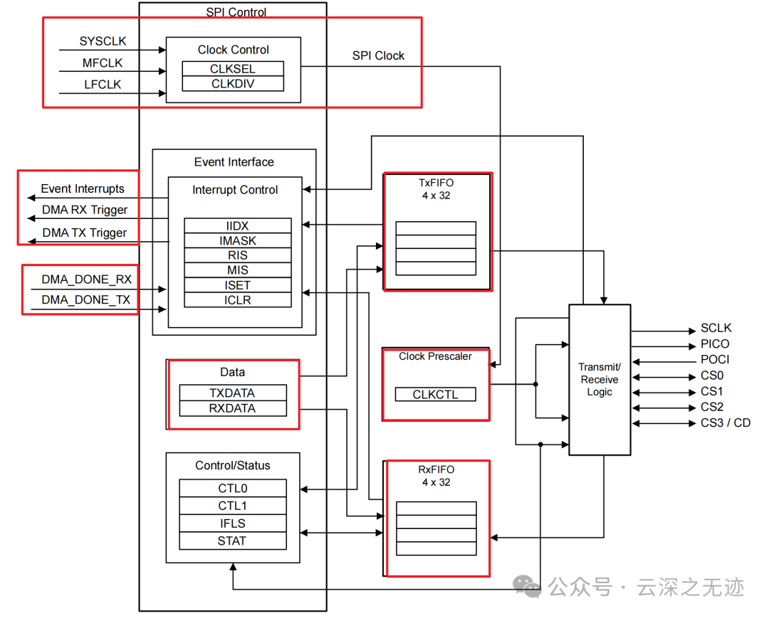
TI has added many peripherals to enhance performance, mainly FIFO for buffering and stitching. The clock sources are abundant, and DMA is also available for both sending and receiving, with notifications upon completion.
Looks nice.
Now let’s discuss some examples:
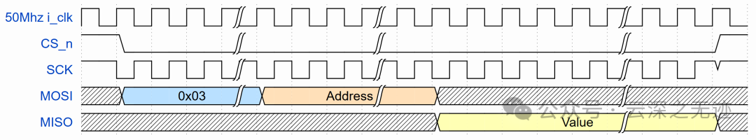
Simultaneous data transmission and reception typically occur when the master device (Master) sends certain commands or data to the slave device (Slave) while the slave also returns status or data to the master.
-
The master sends a “read command” (usually one byte, like 0x03). -
The master continues sending the target memory address (usually 3 bytes, like 0x001234). -
Simultaneously, the slave returns meaningless placeholder data (Dummy Data) while receiving the command and address. -
After the address is sent, the slave will return the data from the memory at the specified address based on the clock signal generated by the master.
Assuming data needs to be read from address 0x001234:
Master sends: 0x03 0x00 0x12 0x34 0xFF 0xFF 0xFF ...Slave returns: 0xXX 0xXX 0xXX 0xXX 0x45 0x67 0x89 ...-
0x03 is the read command.
-
0x00 0x12 0x34 is the address to be read.
-
0xFF is the placeholder data sent by the master to drive the clock.
-
0x45 0x67 0x89 is the valid data returned by the slave. Note that it is provided by the slave.
Let’s look at another example:
-
The master sends a read command (like 0x51, indicating a data block read). -
The master sends the target data block address. -
The master sends several bytes of placeholder data. -
The SD card returns response information while receiving the command and address, and subsequently returns the contents of the data block in the following clock cycles.
Master sends: 0x51 0x00 0x00 0x01 0x00 0xFF 0xFF 0xFF ...Slave returns: 0xFF 0x00 0x00 0x00 0x00 0xFE 0x01 0x02 ...-
0x51 is the read command. -
0x00 0x00 0x01 0x00 is the data block address. -
0xFF is the placeholder data sent by the master to generate the clock. -
0xFE is the SD card data start flag, and the subsequent content is the actual data (0x01 0x02 …).
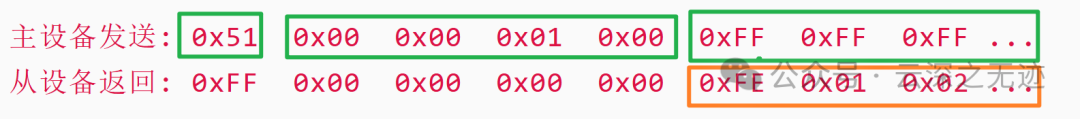
The orange part is what the slave sends out, but the master also needs to send some data.
The data returned by the slave during the first transmission is meaningless:


Because the slave does not know what to expect.
Now, is it very clear?
Here’s an SPI ADC.
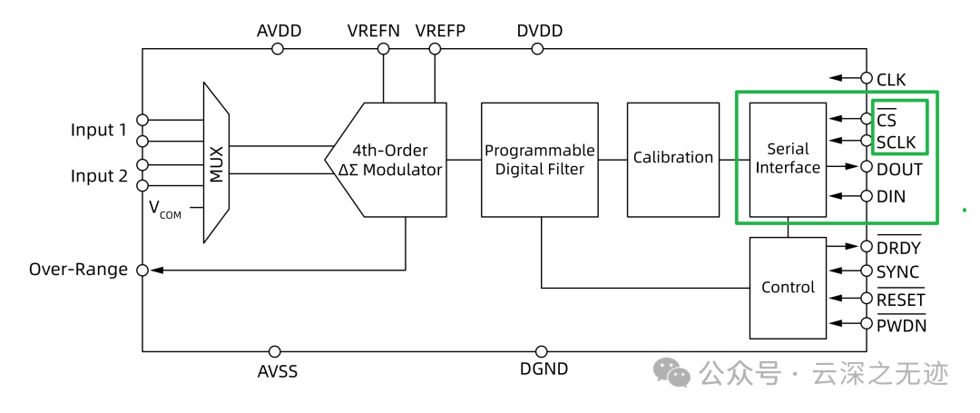
A standard SPI interface.
I like this name.
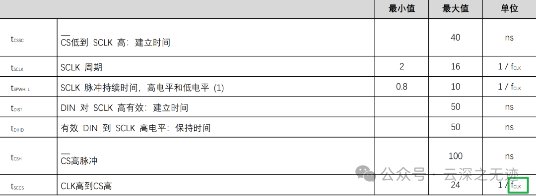
This is timing data.
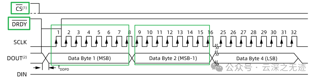
In CLK’s rising edge, data is captured.
MSB is first, 8 bits per byte, forming a data frame.
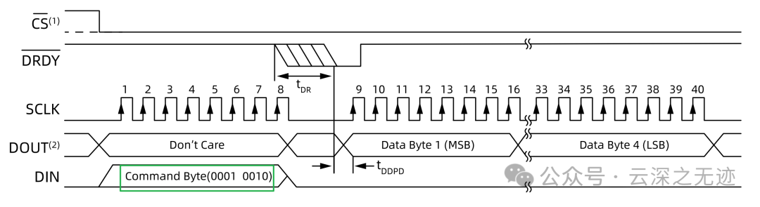
Then look at IN and OUT, indicating the cyclic transmission.
32 bits, 4 bytes are needed to complete one conversion data.

I suddenly realized how data is sent and received:
When CS is pulled low, the slave begins to prepare for transmission. When the master’s clock arrives, the master internally determines bit by bit whether the incoming data is 0 or 1. This data is like dealing cards, transmitted into the master’s internal register. How big is this register? It’s as large as we set it in advance, followed by an interrupt, allowing the CPU or DMA to quickly transfer the data to memory, and then continue with the next one. Bytes of data flow in and out continuously.

Now from the ADC’s perspective, the data sent by the master is DIN, which is for control. The DOUT data will also be sent, but it doesn’t matter.
That’s all for now; meeting adjourned.
https://zipcpu.com/blog/2019/03/27/qflexpress.htmlhttps://dev.ti.com/tirex/explore/node?node=A__ARqjcycmyhag6aCy3n3F4g__MSPM0-ACADEMY-CN__Gx9d9qT__LATESThttps://www.analog.com/cn/resources/analog-dialogue/articles/introduction-to-spi-interface.htmlhttps://www.ti.com/content/dam/videos/external-videos/en-us/10/3816841626001/mspm0-spi-intro.mp4/subassets/mspm0-spi-module-presentation.pdfhttps://www.whxy.com/uploads/files/20241016/CW32L010_UserManual_CN_V1.1.pdfhttps://www.wpgdadatong.com.cn/blog/detail/45539