 Experiment Objective:1. Understand computer storage systems;2. Use Proteus simulation software to draw equivalent circuit diagrams and verify static random access memory (SRAM) chips;3. 6116 memory chip;4. 74LS245 chip, 74LS373 chip.Basic Principle: This experiment aims to verify the static random access memory chip, so the 6116 is selected as the memory chip. The 74LS373 chip is used as the MAR (Memory Address Register) and MDR (Memory Data Register) to store addresses and data, respectively. The 74LS245 chip is used as a tri-state buffer to design the experiment.Experiment Process:1. Select components and chips1) SW-SPDT (Single Pole Double Throw Switch)
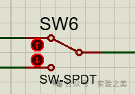 2) Positive terminal, ground
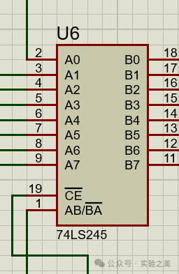
 3) 74LS245 tri-state buffer chipThe 74LS245 is a commonly used digital chip, functioning as a tri-state bus transceiver, typically used for bus level matching issues, allowing for bidirectional data transfer.The 74LS245 also has bidirectional tri-state functionality, allowing it to both output and input data.
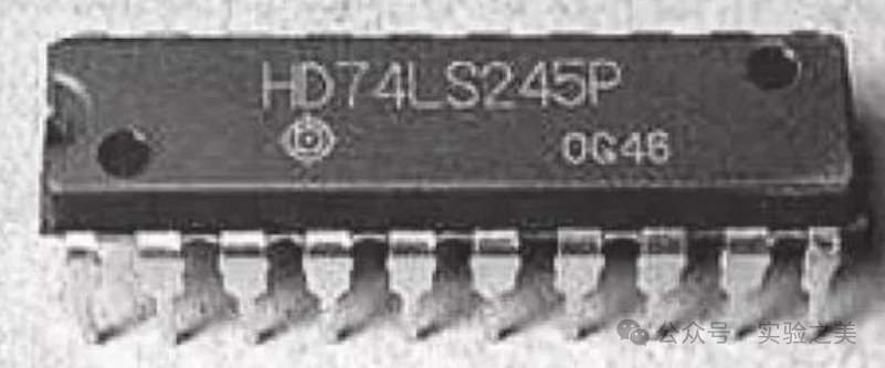 Physical Diagram
A0~A7: A bus terminals
B0~B7: B bus terminals
/CE is low level L, then AB or /BA (DIR): Direction control terminal, high level H means A->B, low level L means B->A.
/CE is low level H, then A and B are both in high impedance state.
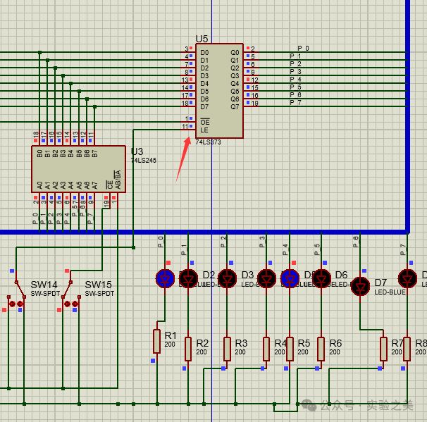
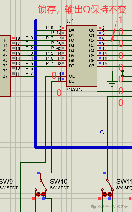
 Circuit Diagram4) 74LS373 chipThe 74LS373 is an 8-bit latch with tri-state output, featuring input data storage, output data driving, and data bus isolation, widely used in digital logic circuits.
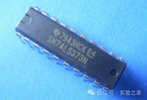 Physical DiagramD0-D7: Data/address input terminals, Q0-Q7: Data/address output terminals.
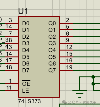
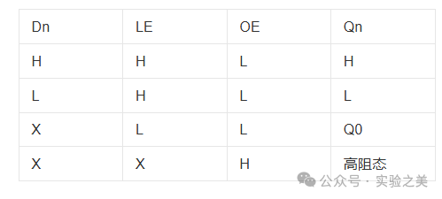 OE is low level, LE (G) is high level, Q=D, transparent state;OE is low level, LE (G) is low level, output Q remains unchanged, latched state;OE is high level, high impedance state5) 6116 static memory chip
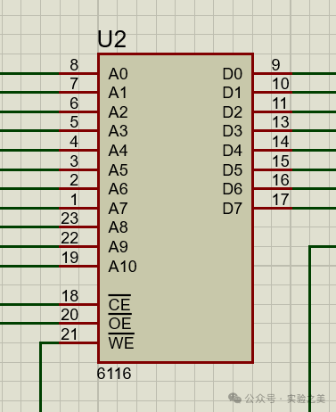
The 6116 is a static memory chip with a data width of 8 bits (8 binary bits) and a capacity of 2048 bytes, packaged in a 24-pin package.
The 6116 chip has 8 bidirectional tri-state data lines D7-D0, where tri-state refers to input state, output state, and high impedance state. The high impedance state means the data line is in a special “disconnected” state; it has 11 address lines A15-A0, indicating 2048 bytes inside the chip, explained as follows.
2048*8=1024*16=16K=2^4*2^10, so there are a total of 16 address lines, 8 indicates there are 8 data lines, 16K*8 memory, and 3 control lines.
1) CE is the selection control signal; when low level, the chip can perform read/write operations; when high level, the chip retains information and cannot perform read/write;
2) WE is the write control signal; when low level, it stores the information on the data line into the memory cell indicated by address lines A10-A0;
3) OE is the output enable control signal; when low level, it reads the data from the memory cell indicated by address lines A10-A0 and sends it to the data bus.
In addition, common static RAMs in the system include 6116, 6264, 62256, etc. In this experiment, the 6116 is used. The 6116 is a 2K╳8 bit static RAM.
 6) Resistors, light-emitting diodes
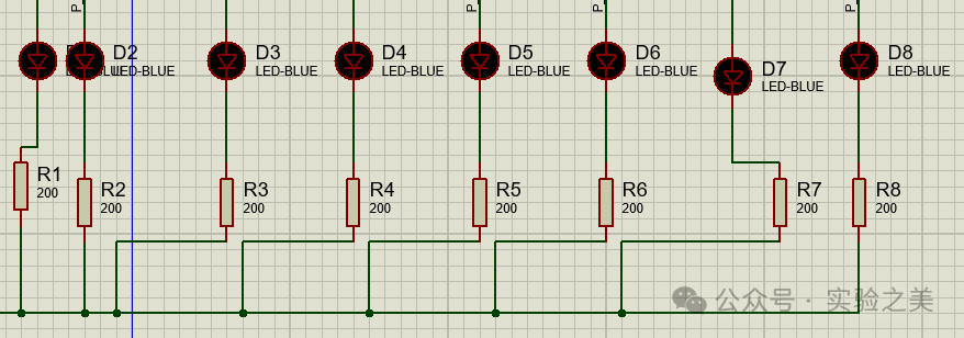 2. Experiment Process1) Draw the circuit diagram
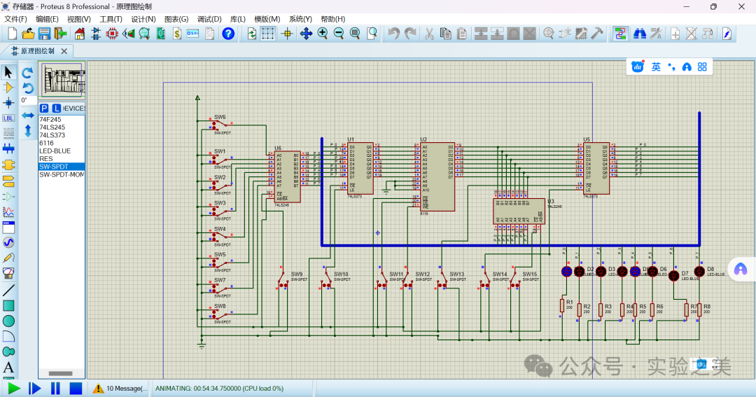
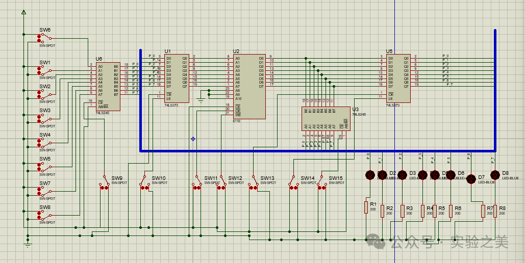 In this experiment, to simplify, only 8 address lines are used, namely A0-A9, while the other A8-A10 are grounded and not used.2) Memory write operation, write hexadecimal data 11H, 12H, 13H, 14H, 15H into storage units 01H, 02H, 03H, 04H, 05H respectively.First, take writing data to storage unit 01H as an example.First, provide the address code by setting the address through high and low levels, for example, set SW7-SW0 to 00000001, turn on the 74LS245 tri-state buffer switch, and send the address to the bus. Then, the 74LS373 acts as the MAR, which is the address register, to store the address. After writing the bus address into the MAR, set the 6116 chip to CE:0, OE:0, WE:0 to write the address to the simulated main memory 6116’s address terminal, thenset the LE terminal of the 74LS373 to 0 to latch.Then, for the corresponding address00000001 of the main memory unit, still using high and low levels to provide the desired storage data (11H, to be stored in00000001 main memory address unit),set SW7-SW0 to 10001000 (11H) to place the data to be saved onto the bus, then switch the 74LS245 switch, i.e., set /CE to:0;set the 6116 chip to CE:0, OE:1, WE:0 to write data, saving it from the data bus through the 74LS245 to the data terminal of the simulated main memory 6116. At this point, the data to be saved is stored in the previously selected address unit.Next, read the just stored 11H data,set the CE of the 74LS245 to 1,set the 6116 chip to CE:0, OE:0, WE:1 to read data, writing it intoMDR, i.e.,74LS373; set LE to 0 to latch, and you can see the just stored 10001000 data displayed through the light-emitting diode.The process is as follows:SW7-SW0 set to 00000001:
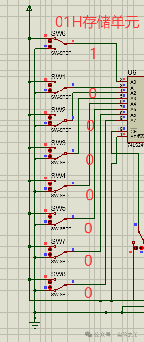 Set 74LS245:If CE is set to high level, A and B are in high impedance state,High impedance state is a common term in digital circuits, indicating that the output state of the circuit is neither high nor low, but presents a high impedance state.
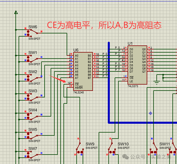 Here, set74LS245 (U6) CE to low level, while AB terminals are high level, A->B mode, so the light on the bus will light up, exactly at address 01H.
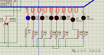 Set 74LS373:First set LE to 1, Q=D, implant the address into 6116, then set LE to 0 to latch the address.
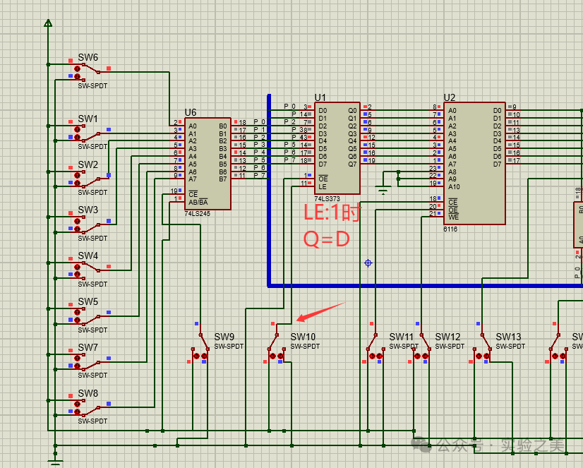
 6116:OE is the output enable control signal, low level, CE is low level, WE is low level,set SW7-SW0 to 00000001 to implant the address.Set SW0-SW7 to 10001000 to write 11H data into the corresponding 00000001 address of 6116, the diode light will light up accordingly.Set74LS245 (U3) CE to low level, while AB terminals are high level, A->B mode, so the light on the bus will light up, exactly at address 01H6116’s OE is the output enable control signal, high level, CE is low level, WE is low level,set SW7-SW0 to 10001000 to store in 6116.
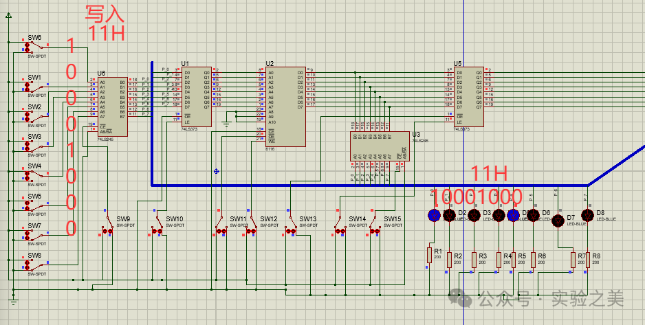 Set74LS245 (U3) CE to high level, data write is complete.
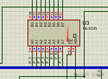 Next, read the value at address 00000001 from the storage unit, and display it using a digital tube.Set SW7-SW0 to 00000001, set LE to high level, Q=D, send the address to 6116 to find the data 01H at that address.6116’s OE is the output enable control signal, low level, CE is low level, WE is high level,set SW7-SW0 to 10001000 to store in 74LS373 MDR.
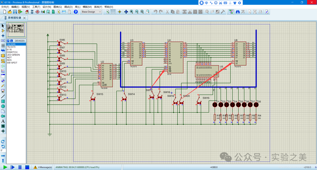 Then set the OE of 74LS245 to L, A->B, read the data from MDR, and display it in the diode, as shown in the figure.