
Source:Learning About Things
Original Author:Long Road Ahead
This article mainly discusses why epitaxial growth technology is the core process of semiconductor manufacturing.
Epitaxial Growth Technology: The Core Process of Semiconductor Manufacturing
As the feature sizes of semiconductor devices continue to shrink, the demand for high-quality thin film materials becomes increasingly urgent. Epitaxial technology, as a commonly used method for growing single-crystal thin films in semiconductor manufacturing, can grow new single-crystal thin films on single-crystal substrates according to the substrate crystal orientation, playing a key role in enhancing device performance. This article will explore the definition, classification, principles, commonly used techniques, and applications of epitaxial technology.In the field of semiconductor manufacturing, as the feature sizes of CMOS devices continue to decrease, the importance of high-quality thin film materials for enhancing device performance has become increasingly prominent. Epitaxial technology, as a key means of growing high-quality single-crystal thin films, provides strong support for the development of the semiconductor industry. By growing epitaxial layers on single-crystal substrates, it is possible to precisely control parameters such as film thickness and doping concentration, while effectively improving device performance, such as enhancing the high-frequency performance of bipolar transistors and addressing latch-up effects in CMOS devices. Therefore, in-depth research on epitaxial technology is of great significance for promoting advancements in semiconductor manufacturing processes.Basic Concepts of Epitaxy1. DefinitionEpitaxy refers to the process of growing a new single-crystal thin film on a single-crystal substrate according to the substrate crystal orientation. The grown single-crystal layer is called the epitaxial layer, and the substrate with the epitaxial layer is referred to as the epitaxial wafer. This growth method allows the epitaxial layer to maintain good consistency with the substrate in terms of crystal structure and orientation, thus providing a high-quality material foundation for semiconductor device manufacturing.2. ClassificationAccording to the type of epitaxial growth material, epitaxy can be divided into homoepitaxy and heteroepitaxy. Homoepitaxy refers to the epitaxial process where the epitaxial layer and substrate materials are the same, such as growing Si on a Si substrate or GaAs on a GaAs substrate. This method can fully utilize the characteristics of the substrate, growing an epitaxial layer that matches well with the substrate lattice, reducing lattice defects and improving the quality of the epitaxial layer. Heteroepitaxy, on the other hand, involves growing an epitaxial layer with a different material from the substrate, such as growing SiGe on Si or GaAlAs on GaAs. Heteroepitaxy provides the possibility of complementary advantages between different materials, allowing for the creation of semiconductor structures with special properties by appropriately selecting the epitaxial layer and substrate materials to meet the needs of different devices.According to the process, epitaxy can be divided into vapor-phase epitaxy (VPE), liquid-phase epitaxy (LPE), solid-phase epitaxy (SPE), and molecular beam epitaxy (MBE). Different epitaxial processes have their own characteristics and applicable ranges, playing different roles in semiconductor manufacturing.According to resistivity, epitaxy can be divided into forward epitaxy and reverse epitaxy. Forward epitaxy involves growing a high-resistivity layer on a low-resistivity substrate (growing lightly doped layers on heavily doped substrates), while reverse epitaxy involves growing a low-resistivity layer on a high-resistivity substrate (growing heavily doped layers on lightly doped substrates). This classification is mainly based on the resistivity differences between the epitaxial layer and the substrate, as different resistivity distributions can significantly impact device performance.According to pressure, it can be divided into atmospheric pressure epitaxy (100 kPa) and low-pressure (reduced pressure) epitaxy (5 – 20 kPa). Pressure has a significant impact on gas transport, chemical reactions, and film quality during the epitaxial growth process. Choosing appropriate pressure conditions can optimize the epitaxial process and improve the quality and uniformity of the epitaxial layer.According to temperature, it can be divided into high-temperature epitaxy (above 1000°C) and low-temperature epitaxy (below 1000°C). Temperature is a key parameter in the epitaxial growth process, directly affecting the rate of chemical reactions, atomic diffusion rates, and the crystal structure and quality of the epitaxial layer. Different epitaxial processes and materials have different temperature requirements, which need to be precisely controlled based on specific conditions.The Importance of Epitaxy in Semiconductor DevicesIn the early days of semiconductor manufacturing, epitaxy was used to improve the high-frequency performance of bipolar transistors. To achieve high-frequency and high-power, the collector of bipolar transistors needs to have a high breakdown voltage and low series resistance; however, these two requirements have conflicting demands on the resistivity of the collector material. Epitaxial technology successfully resolved this contradiction by growing a high-resistivity epitaxial layer (forward epitaxy) on a substrate with very low resistivity. By fabricating bipolar transistors on the epitaxial layer, the high-resistivity epitaxial layer ensures that the transistor has a high breakdown voltage, while the low-resistivity substrate reduces the series resistance, significantly enhancing the performance of high-frequency bipolar devices.In CMOS devices, epitaxy also plays a critical role. In CMOS devices, the parasitic PNP and NPN bipolar transistors can interact, potentially creating a low-impedance path between the power supply and ground, leading to latch-up effects that can damage the device. By adding a low-resistivity epitaxial layer in CMOS devices, it is possible to bypass the emitters of the bipolar transistors, preventing them from turning on and effectively resolving the latch-up effect. Additionally, in advanced CMOS manufacturing processes, the selective epitaxial growth of SiGe is widely used to apply compressive stress to the PMOS device channel, which can enhance the hole mobility and subsequently improve device performance.Basic Principles of Silicon Vapor Phase Epitaxy1. Composition of Epitaxy EquipmentA typical epitaxy system consists of several key components, including a gas distribution system, reaction chamber, a base that supports and heats the silicon wafer, control systems, and exhaust systems. In the gas distribution system, mass flow controllers (MFC) and vacuum valves are used to strictly control the flow of gases into the reaction chamber, ensuring that the reactant gases are delivered accurately and stably to the reaction area. The base is generally made of graphite or polysilicon covered with silicon carbide or silicon nitride, and it needs to have sufficient strength and not react with the reactants and products to ensure stable support and uniform heating of the silicon wafer in a high-temperature, complex chemical reaction environment.2. Reaction SourcesCommon reaction sources for silicon vapor phase epitaxy include silicon tetrachloride (SiCl₄), trichlorosilane (SiHCl₃, TCS), dichlorosilane (SiH₂Cl₂, DCS), silane (SiH₄), and other silanes. Early integrated circuit manufacturing often used silicon tetrachloride (SiCl₄) as a reaction source, but due to its high thermal budget for growing Si epitaxially, it brings many adverse effects. Currently, integrated circuit manufacturing processes require the thermal budget to be as low as possible, so SiCl₄ is mainly applied in traditional epitaxial processes. Trichlorosilane has similar characteristics to SiCl₄ but requires much lower thermal budgets and has higher growth rates, making it suitable for growing thick epitaxial layers. Dichlorosilane is widely used for growing high-quality thin epitaxial layers at lower temperatures, with low defect density, making it a common reaction source for selective epitaxy. The thermal decomposition reaction of silane is a relatively simple chemical reaction in silicon epitaxial growth, represented by the chemical equation SiH₄→Si(s) + 2H₂(g). This process is often used for depositing polysilicon and can also be used for epitaxial growth of very thin layers at temperatures below 900°C, with a rapid deposition rate. Additionally, other silanes such as disilane (Si₂H₆) or trimethylsilane (Si₃H₈) are suitable for depositing very thin epitaxial layers at lower temperatures and have fast deposition rates.3. Epitaxial Growth ModelTo better understand the epitaxial growth process, a detailed epitaxial growth model has been established. In this model, epitaxial growth can be divided into six specific steps: 1. Transport: The reactant gas is transported to the Si surface through gas-phase mass transport. In this step, the reactant gas is delivered to the silicon wafer surface through complex gas dynamics processes, providing the material basis for subsequent reactions.2. Adsorption: Reactants adsorb onto the Si surface. When the reactant gas molecules reach the silicon wafer surface, they interact with the atoms on the surface, attaching themselves through physical or chemical adsorption, preparing for further chemical reactions.3. Chemical Reaction: Reactants undergo chemical reactions on the Si surface, growing the Si epitaxial layer and byproducts. The reactant molecules adsorbed on the silicon wafer surface undergo chemical reactions under high temperature and other conditions, gradually combining silicon atoms to form the epitaxial layer while producing corresponding byproducts.4. Desorption: Byproducts detach from the substrate. The byproducts generated from the reactions need to detach from the silicon wafer surface to make room for new reactions, ensuring the continuity of the epitaxial growth process.5. Escape: The desorbed byproducts escape from the reaction chamber. The byproducts that detach from the silicon wafer surface are expelled from the reaction chamber under the influence of gas flow, preventing the accumulation of byproducts in the reaction chamber that could adversely affect the reaction.6. Incorporation: The generated Si atoms incorporate into the Si substrate lattice points, continuing the Si substrate crystal orientation. The newly generated silicon atoms will orderly join the lattice points according to the crystal orientation of the silicon substrate, thus achieving the growth of the epitaxial layer while maintaining consistency with the substrate crystal orientation.
 During the epitaxial growth process, the epitaxial layer exhibits a characteristic of two-dimensional layer-by-layer growth, which is closely related to the unique “platform-step-kink” structure of the crystal surface. The microscopic structure of the crystal surface can be viewed as composed of flat atomic platforms, steps at the edges of the platforms, and kinks at the corners of the steps. When adsorbed atoms (such as silicon atoms) reach position A on the platform area, if they have low energy and remain stationary, subsequent adsorbed atoms will accumulate around them in a disordered manner, gradually forming short chains of silicon or island structures. As the number of silicon chains or islands increases and they connect with each other, a large number of lattice defects (such as dislocations and stacking faults) can easily be introduced into the crystal surface, severely damaging the single-crystal quality of the epitaxial layer.When the adsorbed atoms have higher energy, they will migrate to lower energy stable positions through surface diffusion mechanisms. Among these, position B at the edge of the step has unsaturated Si-Si bonds, allowing it to form partial covalent bonds with migrating atoms, making its energy state lower than that of position A in the center of the platform, thus becoming the preferred choice for atomic migration. The kink position C at the corner of the step allows atoms to bond with lattice atoms in two directions (completing about 50% of the Si-Si bonds), making its energy state the most stable. Therefore, when atoms migrate to the kink position, they almost no longer undergo secondary migration but directly act as growth nodes, promoting the ordered extension of the epitaxial layer along the substrate crystal orientation. This “platform adsorption – step migration – kink fixation” growth mode is the core mechanism to ensure that the epitaxial layer maintains single-crystal characteristics.Note that if the atomic migration process is suppressed by kinetic factors (such as low temperature or high-speed growth), the growth mode will deviate from the ideal layer-by-layer epitaxy. This is specifically manifested as:Threshold effect of deposition rate: At a specific temperature, there exists a critical deposition rate value. When the actual growth rate exceeds this threshold, the continuously supplied atoms in the gas phase will quickly saturate the surface of the platform, causing many atoms to accumulate disorderly on the platform without having time to migrate to the kink position, ultimately forming polycrystalline or sub-microcrystalline structures; conversely, when the growth rate is below the threshold, atoms have sufficient time to complete surface diffusion, thus achieving single-crystal epitaxy.Temperature control of migration capability: Under fixed deposition rate conditions, temperature plays a key role by affecting the atomic surface migration rate. High-temperature environments can significantly enhance atomic kinetic energy, increasing their diffusion coefficients (for example, the surface migration distance of silicon atoms at 1000°C is more than ten times that at 800°C), allowing for rapid positioning at kink positions to complete ordered growth; while low temperatures can cause atoms to “freeze” at their initial adsorption positions, forcing them to grow in an island mode, ultimately forming polycrystalline films. This temperature-rate synergy forms the core basis for optimizing the epitaxial process window.Factors Affecting Epitaxial Growth Rate1. Reaction SourceThe thermal decomposition behavior and surface reactivity of different silicon sources directly determine the growth rate ranking. Taking common silicon sources as an example:Silane (SiH₄): It can undergo thermal decomposition at low temperatures (600 – 900°C) (reaction: SiH₄ → Si + 2H₂), has a high gas-phase diffusion coefficient (about 0.1 cm²/s), and the Si* active groups produced after decomposition can quickly adsorb onto the substrate surface, resulting in the highest growth rate (up to several μm/min).Halogenated silanes (such as SiCl₄, SiHCl₃): They require higher temperatures (1100 – 1200°C) to release silicon atoms through hydrogen reduction reactions (e.g., SiCl₄ + 2H₂ → Si + 4HCl), and the reaction process is accompanied by the etching effect of HCl byproducts, leading to actual growth rates lower than those of silane.Rate ranking rule: SiH₄ > SiH₂Cl₂ > SiHCl₃ > SiCl₄, this order is negatively correlated with the bond energy of Si-Cl bonds in the silicon sources (SiCl₄ bond energy 3.8 eV > SiHCl₃ bond energy 3.3 eV), the higher the bond energy, the more energy is required to break the chemical bonds, resulting in a decrease in reaction rate.2. TemperatureTemperature controls the rate-limiting steps of the reaction, causing the epitaxial growth to exhibit dual-region characteristics:High-temperature region (mass transport control region):At this time, the surface chemical reaction rate is extremely fast, and the gas-phase diffusion of silicon source molecules becomes the rate-limiting step. The growth rate mainly depends on the diffusion flux of the reactant gas through the boundary layer (thickness δ≈0.1 – 1 mm), which can be described by Fick’s law:
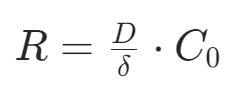 Where D is the diffusion coefficient, and C₀ is the gas-phase bulk concentration. Since the diffusion coefficient has a weak dependence on temperature (D ∝ T^(3/2)), the growth rate in the high-temperature region is not sensitive to temperature fluctuations but is highly sensitive to the geometric structure of the reaction chamber (such as gas inlet design, substrate spacing) and gas flow velocity (Reynolds number Re).Low-temperature region (surface reaction control region):The thermal decomposition efficiency of silicon source molecules decreases, and surface chemical reactions become the rate-limiting step. The growth rate follows the Arrhenius law:
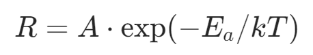 Where the activation energy Eₐ (for example, Eₐ≈2.3 eV for the hydrogen reduction reaction of SiCl₄) determines temperature sensitivity.When preparing thick epitaxial layers (such as high-resistivity drift layers for power devices), high-temperature region processes are preferred to achieve uniform growth using the stability of mass transport control; when growing nanoscale ultra-thin epitaxial layers (such as FinFET source-drain strain layers), low-temperature region processes are used to achieve atomic-level thickness control through precise temperature control, but care must be taken to suppress the tendency for polycrystallization.3. Reactant ConcentrationTaking SiCl₄ as an example, the epitaxial process is mainly divided into two processes: the first process is the hydrogen reduction of SiCl₄, and the second process is the growth of the Si epitaxial layer. The growth rate of silicon epitaxy is determined by the slower of these two processes. When the concentration of SiCl₄ is low, the hydrogen reduction of SiCl₄ is limited, and the rate of the oxidation-reduction reaction releasing silicon atoms is far less than the rate of orderly arrangement of silicon atoms on the substrate to grow single-crystal silicon, thus the surface oxidation-reduction reaction rate controls the growth rate of the epitaxial layer, which is a type of surface chemical reaction-controlled growth. As the concentration of SiCl₄ increases, the oxidation-reduction reaction rate accelerates, and the epitaxial growth rate also increases accordingly. When the concentration reaches a certain level, the rate of the oxidation-reduction reaction releasing silicon atoms will exceed the rate of orderly arrangement of silicon atoms on the substrate to grow single-crystal silicon, at which point the control shifts from oxidation-reduction reaction rate to the rate of orderly arrangement of silicon atoms, making it easier to generate polycrystalline silicon. When the concentration of SiCl₄ exceeds 0.1, the epitaxial growth rate will gradually decrease because the grown silicon film is etched by the byproduct HCl at high temperatures, leading to a “reverse reaction.” When the concentration of SiCl₄ exceeds 0.27, only the HCl etching reaction on the silicon film exists.4. Gas Flow RateSimilar to CVD processes, the gas flow rate in the epitaxy chamber also affects the deposition rate. The higher the gas flow rate, the thinner the boundary layer, and the reactants in the chamber can more easily diffuse through the boundary layer to reach the substrate surface, resulting in a faster epitaxial growth rate. However, when the gas flow becomes too high, the boundary layer becomes very thin, and the number of reactants diffusing to the substrate surface exceeds the amount needed for surface chemical reactions at the epitaxy temperature, at which point the epitaxial growth shifts to being controlled by the surface chemical reaction rate, and the growth rate of the epitaxial layer does not significantly increase with the gas flow rate.5. Crystal PlaneDifferent crystal planes have different covalent bond densities, and their bonding capabilities vary, which can also affect the growth rate. In crystal planes with low covalent bond density, such as the (111) plane, the bonding capability is poor, resulting in a slower epitaxial growth rate; conversely, in crystal planes with high covalent bond density, such as the (100) plane, the bonding capability is strong, leading to a faster epitaxial growth rate.Common Epitaxial Techniques1. Reduced Pressure Chemical Vapor Deposition (RPCVD)Atmospheric pressure epitaxy, as a relatively mature epitaxial process, has gradually exposed some issues against the backdrop of continuously improving semiconductor manufacturing levels, such as excessive drift of epitaxial patterns and diffusion of impurities from buried layers into the epitaxial layer. RPCVD, as a low-pressure epitaxy technology (1×10³ – 2×10⁴Pa), can effectively address these issues. Using low-pressure epitaxy technology can reduce self-doping effects because, under low pressure, the average free path of molecules increases, accelerating the diffusion rate of impurities, allowing impurities escaping from the substrate to quickly pass through the boundary layer and reducing the chances of re-entering the epitaxial layer, effectively lowering the impact of self-doping on impurity concentration and distribution in the epitaxial layer, achieving steep impurity distributions. Additionally, RPCVD can improve the uniformity of the epitaxial layer’s resistivity, reducing the drift and distortion of buried layer patterns. Compared to atmospheric pressure epitaxy, the growth rate of low-pressure epitaxy only decreases by 15% – 17%, but the epitaxial growth temperature can be lowered by 100 – 150°C, significantly improving pattern transfer and the quality of buried layers.2. Selective Epitaxy (SEG)Silicon selective epitaxy utilizes the characteristic that silicon is difficult to nucleate and continue growing into a thin film on insulators, allowing for selective growth of epitaxial layers in specific areas on the silicon surface while not growing in other areas. The likelihood of nucleation of silicon on SiO₂ is minimal, while it is maximal on Si, because the Si nucleus/SiO₂ interface generates significant lattice mismatch energy compared to the homoepitaxial nucleation of Si nucleus/Si substrate. Additionally, the areas where epitaxial growth is desired are usually within windows or depressions on the silicon surface, where nucleation energy is lower, thus atoms landing on SiO₂ are less likely to nucleate and migrate to the more favorable nucleation sites on the silicon surface depressions. In advanced CMOS manufacturing, selective epitaxy can be used for strain engineering of conductive channels by selectively growing SiGe in the source-drain regions of devices to increase the compressive stress on the conductive channel, thereby enhancing the hole mobility of PMOS, or selectively growing high-mobility channel materials such as Ge or InGaAs in trenches.3. Lateral Overgrowth Epitaxy (ELO)Lateral overgrowth epitaxy is an epitaxial technique developed based on selective epitaxy. When the thickness of the epitaxial layer grown by silicon selective epitaxy exceeds the step height of the SiO₂ island, it will grow laterally in addition to vertically along the silicon substrate surface. This epitaxial technique is called lateral overgrowth epitaxy (ELO). The ratio of lateral to vertical growth rates is influenced by factors such as the height of the window or step and the substrate crystal orientation. By controlling these factors, it is possible to regulate the lateral and vertical growth rates, thereby obtaining epitaxial layers with specific structures and properties.4. Molecular Beam Epitaxy (MBE)Molecular beam epitaxy involves evaporating the components of the epitaxial layer in ultra-high vacuum, forming atomic or molecular vapor streams that reach the heated substrate surface, thereby forming the epitaxial layer. MBE can grow elemental semiconductors such as Si and Ge, as well as compound semiconductors like SiGe, GaAs, and GaN single crystals. A typical MBE system consists of ultra-high vacuum systems, growth systems, measurement, analysis, and monitoring systems. Compared to other epitaxial techniques, MBE has characteristics such as slower and controllable growth rates, smooth surfaces and interfaces, and relatively low epitaxial temperatures. The lower growth rates allow molecules or atoms sufficient time to reach nucleation points, thus producing high-quality thin films. The relatively low epitaxial temperatures reduce system outgassing, minimize diffusion effects and self-doping effects, and decrease the redistribution of impurities from the substrate and the generation of thermal defects. Solid-state MBE uses solid-source ultra-high vacuum evaporation technology, which allows for precise control of the chemical composition and doping concentration of the thin film compared to ordinary thermal evaporation technology, and enables atomic-level precise control of thickness. Due to these advantages, MBE is widely used for growing abrupt heterojunctions and complex multilayer structures with steep compositional and doping distributions, including quantum well devices, superlattices, and lasers, all benefiting from precise control of composition during the epitaxial growth process. For example, MBE technology can produce many superlattice epitaxial layer structures composed of alternating GaAs and AlGa₁₋ₓAs with thicknesses as low as 10Å. MBE is not only important in the semiconductor field but also has applications in other areas such as optics, where components like bus station announcement boards and large displays in sports arenas are often manufactured using MBE.