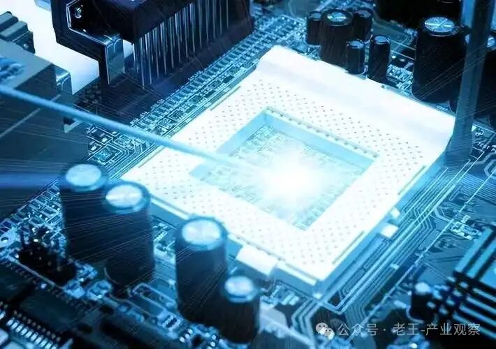
In the context of increasingly fierce global competition in the semiconductor industry, China’s semiconductor sector is advancing at a remarkable pace. Recently, a series of semiconductor projects have sprung up across China, covering key areas such as chip manufacturing, packaging and testing, and equipment R&D. These projects are significant markers of China’s move towards high-end and independent semiconductor production. Their concentrated advancement not only injects strong development momentum into China’s semiconductor industry but also indicates that China’s position in the global semiconductor supply chain will be further enhanced.
1. Chip Manufacturing: Capacity Expansion and Technological Upgrades
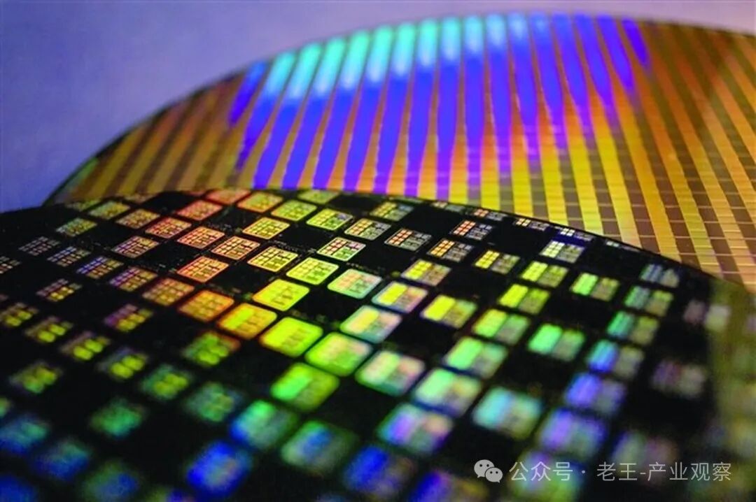
In the field of chip manufacturing, several projects demonstrate China’s determination to enhance capacity and break through advanced process technologies. Jiangsu Superchip Semiconductor Co., Ltd. has completed the relocation of its new factory and is about to fully commence mass production of 8-inch silicon carbide (SiC) single crystal substrates, planning to increase the annual output of 6-8 inch SiC substrates to 1.5 million pieces. As a key foundational material for chip manufacturing, larger SiC substrates yield more chips at lower costs, with the industry currently transitioning from 4-inch and 6-inch to 8-inch substrates. In addition to Superchip, several Chinese manufacturers such as Tianyue Advanced and Tianke Heda have made progress in the 8-inch SiC materials segment. With the release of capacity, the cost of SiC chips is expected to decrease, accelerating their market application.
In Beijing, Ruineng Microelectronics (Beijing) Co., Ltd. has completed all construction work for its “6-inch automotive-grade power semiconductor wafer production base project,” which has passed completion acceptance and is expected to officially start production in June 2025, with an annual capacity of 120,000 wafers to meet the demand for power semiconductors in automotive electronics and other fields.
2. Packaging and Testing: Enhancing Back-End Competitiveness
Packaging and testing are crucial back-end processes in the semiconductor industry, and several projects have recently been launched. The Nantong Kangyuan Integrated Circuit Packaging Substrate Project, invested and constructed by Dongguan Kangyuan Electronics Co., Ltd., has a total investment of 5 billion yuan. This project specializes in producing key materials for the integrated circuit industry chain, effectively addressing the “bottleneck” technical challenges in the integrated circuit industry and helping to build a new generation of information technology industry cluster in Nantong, with production imminent.
Additionally, the Jiashan Economic and Technological Development Zone has signed a cooperation agreement with Shanghai Nanxin Semiconductor Technology Co., Ltd. to establish a packaging and testing base for automotive-grade chips in Jiashan, with a planned total investment of 1 billion yuan in the first phase. Shanghai Nanxin Semiconductor is a leading listed company in the domestic power analog chip industry, gradually expanding into automotive electronics and industrial fields. The launch of this project will enhance its packaging and testing capabilities in the automotive-grade chip sector.
3. Equipment R&D: Breaking Through Key Equipment Technology Bottlenecks
Semiconductor equipment is the cornerstone of industry development, and China is actively laying out in equipment R&D. On February 5, the Qingdao West Coast New Area Management Committee signed an investment cooperation agreement with Haichuang Intelligent Equipment (Yantai) Co., Ltd. for a semiconductor equipment R&D and production headquarters project with a total investment of 1 billion yuan, which will develop and manufacture products such as wafer-level permanent bonding, temporary bonding, and debonding equipment. Haichuang Intelligent Equipment is targeting both international and domestic markets, committed to the R&D, manufacturing, and sales of high-end semiconductor equipment, with all products benchmarked against international advanced levels.
On January 26, the signing of the TGV glass substrate semiconductor process equipment R&D and industrialization project and the glass substrate PVD coating equipment R&D and production project took place in the Jiuguan Semiconductor Optoelectronic Industrial Park in Nanxun District. Suzhou Jingzhou Equipment Technology Co., Ltd. is currently the only advanced manufacturing enterprise in China capable of providing large-size complete line wet supply. After the project is put into production, it will achieve an annual production capacity of 150 sets of TGV glass substrate semiconductor process equipment. Anhui Yuehao Electronic Equipment Co., Ltd. will establish a glass substrate PVD coating equipment R&D and production base. The landing of these two high-end semiconductor equipment import substitution projects will promote the localization process of semiconductor equipment in China.
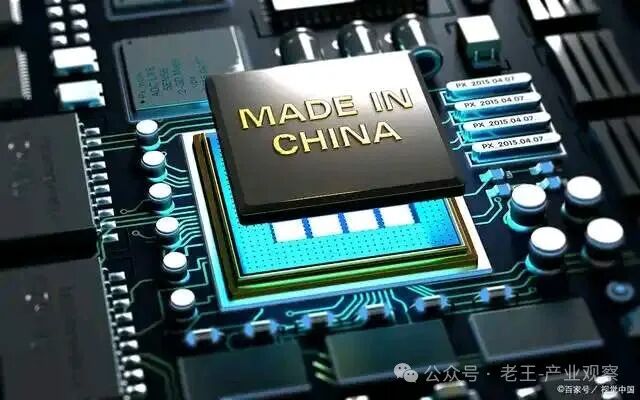
The recent concentration of new semiconductor projects in China is a positive signal for industry development. From chip manufacturing to packaging and testing, to equipment R&D, the collaborative development of various links will help improve China’s semiconductor supply chain and enhance the overall competitiveness of the industry. Although challenges remain in technology and talent, with the gradual advancement and implementation of these projects, China’s semiconductor industry is expected to occupy a more important position in the global market, achieving a transformation from a major semiconductor country to a strong semiconductor nation.