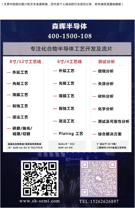
Senhui Introduction: Suzhou Senhui Semiconductor, supported by a strong research and technology team, focuses on providing complete process solutions and wafer fabrication services for global compound semiconductor customers. The company team members have been deeply involved in the semiconductor industry for many years, possessing decades of rich experience in photolithography, thin film processes, epitaxy, bonding processes, as well as etching, wet processing, and polishing development and manufacturing capabilities, with mature technology and extensive process experience.
Content:
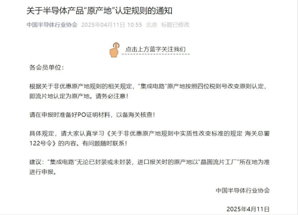
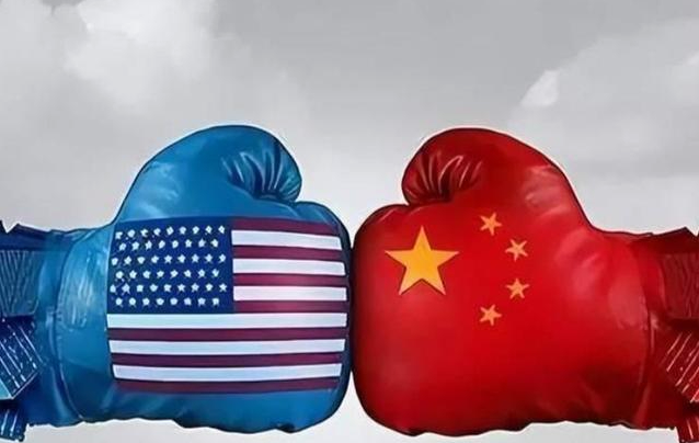
Against the backdrop of a deep restructuring of the global semiconductor supply chain, the China Semiconductor Industry Association issued an “Emergency Notice on the Rules for Determining the Origin of Semiconductor Products” on April 11, 2025, marking a key step in China’s governance of the semiconductor industry.
The new regulations establish a dual identification mechanism through “four-digit tariff code changes + wafer fabrication location locking,” anchoring the origin of integrated circuits at the wafer manufacturing stage. This is not only a technical adjustment for customs supervision but also a proactive upgrade of the national industrial strategy.
Policy Origins and Rule Reconstruction
The global semiconductor industry has long exhibited a cross-regional segmented layout, with core processes such as design and development, wafer manufacturing, and packaging testing dispersed across different jurisdictions. The ambiguity of the current origin attribution determination mechanism directly leads to multiple governance challenges, including disputes over export tax rebate qualifications, conflicts in customs tariff classification, and inaccurate assessments of supply chain security risks.
Comparison of International Origin Determination Frameworks
– “Complete Origin Standard”: Applicable to mineral and other natural resource products
– “Value-Added Ratio Standard”: The EU applies a 45% value-added threshold for electronic products
– “Process Standard”: The US applies a dual identification of “design + key manufacturing” for semiconductors
– “China’s New Regulations”: Creatively integrates CTC (tariff code change) and process standards, establishing the “pre-process determinism”
Three-Dimensional Perspective on Regulatory Upgrades
1. “Technical Sovereignty Dimension”: Incorporating advanced processes of 28nm and below into strategic material control
2. “Trade Compliance Dimension”: Requiring enterprises to establish a full-process management system for “wafer fabrication traceability – customs declaration – compliance review”
3. “Supply Chain Reconstruction Dimension”: Guiding design companies to establish deep binding with domestic foundries
|
Issue Domain |
Traditional Model |
Risks After New Regulations Implementation |
|
Export Tax Rebate |
Apply for tax rebate based on packaging location |
Need to re-audit the process proportion of wafer fabrication location |
|
Anti-Dumping Investigation |
Determined by the registration location of the design company |
Need to submit proof of foundry process nodes |
|
Evading Technology Blockades |
Through transshipment trade via third countries |
Facing penetration checks of wafer fabrication equipment’s original location |
Detailed Explanation of Technical Identification Standards
According to the implementation rules of “General Administration of Customs Order No. 122”, semiconductor products are subject to the “8542 tariff breakthrough” principle:
|
Processing Stage |
Tariff Changes |
Origin Weight |
|
EDA Design |
No tariff code change |
0% |
|
Wafer Fabrication |
Change from blank wafer (7006) to chip (8542) |
100% |
|
Packaging Testing |
Maintain 8542 tariff code |
0% |
Decomposition of Wafer Fabrication Process Technical Weight
Photolithography (25%) + Thin Film Deposition (18%) + Ion Implantation (15%) + Metallization (12%) constitute the four core technology nodes, contributing a total of 70% to the origin determination weight. It is particularly noteworthy that processes below 7nm involving EUV lithography will trigger additional review mechanisms due to their complexity.
Enterprise Compliance Operation Guidelines
In response to the implementation of the new regulations, it is recommended that enterprises establish three major response systems:
1. “Supply Chain Visualization System”: Integrating foundry order data with customs systems
2. “Dual-Track Wafer Fabrication Strategy”: Implementing a “domestic backup production line” plan for sensitive processes
3. “Customs Advance Ruling Mechanism”: Applying for advance ruling for multi-country wafer fabrication projects