Mobile chips, solar panels, LED lights… these technological products that change our lives are all fundamentally reliant on semiconductors. In the world of semiconductors, the most basic and crucial “partners” are N-type and P-type semiconductors. They are like a pair of complementary partners, working together to support the operation of modern electronic devices. Today, let’s break down the core differences between these two types of semiconductors in the simplest terms.
First, let’s understand: Why do semiconductors need to be “doped”?
Pure semiconductors (like silicon and germanium) have very weak conductivity, akin to a “half-blocked wall” where electrons struggle to pass through. However, by adding a small amount of specific “impurities”, their conductivity can instantly “skyrocket”—this process is called “doping”, and N-type and P-type semiconductors are the two core forms after doping.
The key principle is simple: changing the type and quantity of “charge carriers” through impurities. Here, the “charge carriers” refer to the “particles” responsible for conductivity in semiconductors, mainly electrons (negatively charged) and “holes” (which can be understood as “vacancies left by electrons”, effectively positively charged).
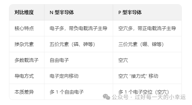
N-Type Semiconductor: The “Electron-Rich” Negative Charge Carrier
The “N” in N-type semiconductor comes from the English word “Negative”. Its core characteristic is that it has a particularly high number of free electrons.
The doping involves “five-valent elements”: such as phosphorus (P) and arsenic (As). These elements have five electrons in their outermost shell, while silicon atoms have only four.
The doping process is like “adding one extra electron”: when a phosphorus atom replaces a silicon atom, it forms four chemical bonds with surrounding silicon atoms, using up four electrons, and leaving one “extra” electron. This electron is almost unbound and can easily become a free electron, moving freely within the semiconductor.
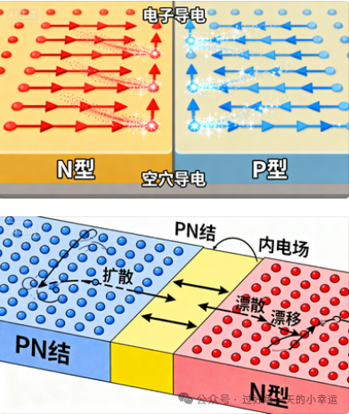
Conductivity relies on “electron charge carriers”: in N-type semiconductors, free electrons are the “majority carriers” (the primary source of conductivity), while holes are the “minority carriers” (with very low presence). The formation of current essentially involves these free electrons moving collectively in one direction.
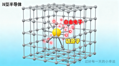
In simple terms, N-type semiconductors are like an “electron supermarket”, filled with a large number of free electrons waiting to “work”, resulting in high conductivity.
P-Type Semiconductor: The “Electron-Deficient” Hole Carrier
The “P” in P-type semiconductor comes from the English word “Positive”. Its core characteristic is that it has a particularly high number of holes.
The doping involves “three-valent elements”: such as boron (B) and gallium (Ga). These elements have only three electrons in their outermost shell.
The doping process is like “digging a vacancy”: when a boron atom replaces a silicon atom, it needs to form four chemical bonds with surrounding silicon atoms, but only has three electrons available, thus leaving behind an “electron vacancy”—this is the hole.
Conductivity relies on “hole relay”: in P-type semiconductors, holes are the “majority carriers”. Surrounding electrons continuously fill these holes, while the holes move in the opposite direction of the electrons, effectively conducting positive charge.
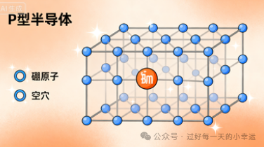
If N-type is “electron-rich”, then P-type is “hole-rich”, completing conductivity through the “relay race” of electrons and holes.
Core Differences Overview (Easy to Understand)
Key Reminder: They are both “neutral”!
Many people mistakenly believe that N-type carries negative charge and P-type carries positive charge, but that’s incorrect! The doped semiconductors remain electrically neutral overall!
This is because the impurity atoms themselves are neutral: in N-type, when phosphorus atoms lose one electron, they become positively charged ions, but the negative charge of free electrons cancels out this positive charge; in P-type, when boron atoms gain one electron, they become negatively charged ions, while the positive charge of holes cancels out this negative charge. It’s like a “balance sheet” overall, just that the “main characters” of conductivity have changed internally.
Why are these “CPs” indispensable?
Individually, N-type or P-type semiconductors, no matter how strong their conductivity, cannot play a significant role. However, when they are “joined together” to form a PN junction, miracles happen—PN junctions are the core foundation of diodes, transistors, and chips, enabling key functions like “unidirectional conductivity” and “signal amplification”.
For example, a diode relies on the PN junction to allow current to flow only from P-type to N-type; and the countless transistors in chips are essentially clever combinations of PN junctions, ultimately achieving complex functions like computation and storage. Without the combination of N-type and P-type, there would be no electronic era today!
In Summary
N-type semiconductor: “rich in electrons, conducts electricity through electrons”; P-type semiconductor: “rich in holes, conducts electricity through holes”. They are the “positive and negative partners” in the semiconductor world, becoming the “foundation stone” of all electronic devices through simple doping modifications.
The next time you see a mobile phone or computer, think about this: the core of these black technologies is actually these two “complementary character” semiconductors working silently!