Reading Good Books Together
1. Overview of Power Semiconductor Modules
Let’s start by discussing the basic structural layers of traditional power modules:
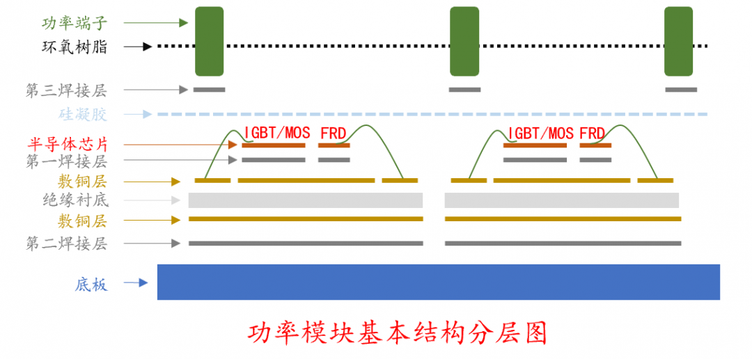
As we can see, many of the semiconductor chips we discussed earlier are just a part of the power module, which also includes other components. The selection and combination of these components, along with the characteristics of the semiconductor chips, will determine the overall performance of the power module.
❖ Power Semiconductor Chips: Such as IGBT, FRD, MOSFET, etc., including traditional Si-based and emerging third-generation semiconductors like SiC. Their characteristics are constrained by their design and also depend on the packaging materials and technologies used;
❖ Insulating Substrate: Mainly composed of ceramic or silicide insulating layers, covered with metal layers made of gold, silver, and copper;
❖ Base Plate: Generally made of copper, copper alloys, carbon-based reinforced mixtures, silicon carbide aluminum, etc.;
❖ Interconnection Materials: Generally divided into lead solder and lead-free solder, also including emerging technologies like silver sintering and solid-liquid interdiffusion connections;
❖ Power Interconnection: Mainly uses aluminum wire bonding, as well as crimp connections and power terminal connections;
Each layer of the power module is closely related, possessing different electrical, mechanical, and thermal properties. Design considerations must account for their compatibility, and different combinations can be generated based on various application scenarios. Therefore, many semiconductor module manufacturers will choose different materials according to different application requirements.
When selecting packaging materials for power modules, the following factors are generally considered:
★ Thermal Characteristics
★ Electrical Characteristics
★ Mechanical Characteristics
★ Chemical Characteristics
★ Cost
★ Technological Maturity
Among these, thermal performance is the most critical factor. The most considered aspect during the selection and use of power modules is also thermal management, and the primary cause of failure is thermal issues; thus, thermal characteristics are the main consideration in the selection of power modules.
Thermal Stress: During temperature cycling and thermal fatigue testing, the differing thermal expansion coefficients of materials in each layer will lead to thermal stress. If it exceeds the mechanical strength limit of a certain layer, failure will occur;
Thermal Conductivity: During operation, semiconductor chips will generate a significant amount of thermal loss, which needs to be effectively dissipated through the substrate and base plate to ensure that the junction temperature of the chip remains within an acceptable range. Generally, a lower junction temperature can extend the reliability of the module; for every 9°C increase in junction temperature, the failure probability of the module will double.
Therefore, the design of power modules, aside from the semiconductor chips, also requires careful selection and design of other components.
The insulating substrate primarily serves as the base for the semiconductor chip, and conductive materials, insulating materials, and resistive materials are deposited on the insulating substrate, which can also form passive components. As a mechanical support structure for the power module, it needs to withstand different working environments and must have sufficient thermal conductivity to quickly transfer heat generated by the chip. Additionally, some subsequent processes, such as thin films, bonding, spacing, etc., require the insulating substrate to have reasonable flatness.
2. Power Semiconductor Module – Insulating Substrate
Selection Criteria for Power Module Substrates
Electrical Characteristics
High resistivity: >1012Ω/cm
High dielectric strength: >200V/mil (1mil=0.0254mm)
Low dielectric constant: <15
Thermal Characteristics
High thermal conductivity: Effective thermal conduction >30W/m·K
Thermal expansion coefficient that matches the semiconductor chip: Generally selected in the range of
2~6×10⁻⁶/℃
High temperature resistance: Generally able to meet the maximum temperature of subsequent processing technologies
Mechanical Characteristics
High tensile strength: >200MPa
High flexural strength: >200MPa
Reasonable hardness
Machinability: Easy to grind, polish, cut, and drill
Metalizable: Suitable for common metallization techniques, such as thin film and thick film processes, electroplating, etc. We will discuss this in the next article.
Chemical Characteristics
Corrosion resistance to acids, bases, and other process solutions
Low water absorption, small voids
Non-toxic
Will not ionize
Density
Low density: Minimizes mechanical shock
Maturity
Technology is relatively mature
Material supply can meet demand
Cost should be as low as possible (it is more appropriate to say cost-performance ratio, as different applications allow for different cost tolerances)
Currently, several insulating substrate materials suitable for power semiconductor devices include the following:
❖ Ceramic Materials (3 types): Al2O3 (96%, 99%), AlN, BeO
❖ Silicon-based Substrates: Si3N4
Among these, alumina is the most common, but when the framework for power semiconductor chips is determined, some suppliers will adjust other components in the module to meet requirements, so AlN and Si3N4 are also considered common. Next, let’s discuss the advantages and disadvantages of these insulating substrate materials.
 1. Alumina (Al2O3)
Advantages:
It is the most commonly used insulating substrate material, with relatively mature processes; low cost; performance can meet the above requirements;
Disadvantages:
Low thermal conductivity, thermal expansion coefficient (6.0~7.2×10⁻⁶/℃) not well matched with semiconductor chips (generally 2.8×10⁻⁶/℃); high dielectric constant; average acid corrosion resistance;
Therefore, alumina is suitable for medium and low power devices; suitable for high voltage and low-cost devices; suitable for sealed packaging; 99% alumina has a better cost-performance ratio.
2. Aluminum Nitride (AlN)
Advantages:
High thermal conductivity, about 6 times that of Al2O3, suitable for high power semiconductor applications; AlN’s thermal expansion coefficient is 4.6×10⁻⁶/℃, which matches well with chips; performance also meets the above requirements;
Disadvantages:
It is a relatively new material, but its process is not as mature as alumina and beryllium oxide; it is difficult to directly coat copper on its surface, which can easily lead to thermal fatigue failure; cost is about 4 times that of alumina; and it may decompose into hydrated alumina at high temperatures and high humidity;
It is one of the ideal substrates for high power semiconductor devices, but due to its average mechanical fracture strength, it needs to be used in conjunction with a metal base plate.
3. Beryllium Oxide (BeO)
Advantages:
Extremely excellent thermal conductivity, about 8 times that of Al2O3; also suitable for high power semiconductor applications; mature processes;
Disadvantages:
Both solid and gaseous forms are toxic; relatively high thermal expansion coefficient, about 7.0×10⁻⁶/℃; poor mechanical strength, only about 60% of Al2O3; cost is 5 times that of alumina;
The toxicity greatly limits the use of this material.
4. Silicon Nitride (Si3N4)
Advantages:
Thermal expansion coefficient is about 3.0×10⁻⁶/℃, which is close to that of semiconductor chips; superior mechanical properties: more than twice that of Al2O3 and AlN, three times that of BeO; high thermal conductivity, 2.5 times that of Al2O3; suitable for high power semiconductor applications; high temperature strength and excellent thermal shock resistance;
Disadvantages:
Technology is still relatively immature, so suppliers are also limited; not suitable for applications in acidic environments; cost is 2 to 2.5 times that of Al2O3;
For applications in high power semiconductor devices, Si3N4 should be the optimal substrate material currently available, with advantages in CTE and thermal conductivity, and high reliability.
Among the above four insulating substrates, the most common is alumina, the least common is beryllium oxide, and the relatively superior is silicon carbide. Many manufacturers are pairing different insulating substrates for different applications, which can indirectly enhance the performance of existing chips as chip technology develops.
3. Power Semiconductor Module – Insulating Substrate Metallization
Several Common Metallization Techniques:
❖ Thin Film
❖ Thick Film
❖ Electroplated Copper
❖ Direct Copper Bonding
❖ Activated Soldering Copper Coating
❖ Conventional Hard Soldering Copper Coating
Requirements for Metallization of Insulating Substrate Surfaces:

Thermal Characteristics:
High thermal conductivity (>200W/K·m)
Thermal expansion coefficient matching with the insulating substrate
High thermal fatigue resistance (temperature cycling related)
High thermal stability (i.e., high-temperature resistance)
Electrical Characteristics:
Strong current-carrying capacity
Low resistivity (generally, the voltage drop across the metal coating should be less than 1/10 of the saturation voltage drop between the chip’s collector and emitter)
Mechanical Characteristics:
High adhesion to the insulating substrate
Suitable for bonding
Suitable for soldering and other processes
Compatible with the insulating substrate
Compatible with existing process equipment
Chemical Characteristics:
Easy to etch into shape (thick film does not require this)
Does not react with solvents during processing
Non-toxic
Good corrosion resistance
Chemically inert
Cost:
As low as possible while meeting requirements (this is unquestionable)
 Thin Film Technology
Thin films are generally formed by sputtering or physical vapor deposition over the entire surface of the substrate. The thin film layer is obtained through encapsulation materials, exposure, etching, etc. Common thin film metal materials include: gold, silver, copper, and aluminum.
Compared to thick film technology, thin film technology can achieve more precise positioning and smaller spacing, making it very suitable for high-frequency, high-density applications. The bonding strength between the thin film layer and the insulating substrate is strong, and it has excellent resistance to thermal fatigue aging, while its bonding capability is also superior to thick film technology; however, from a cost perspective, thin film technology is about 5 times more expensive than thick film technology, and multi-layer thin film structures are more challenging.
Typically, the thickness of thin film layers is 2.5um, and it can be even thinner, with current-carrying capacity ranging from several to dozens of amperes.
Thick Film Technology
Thick films are generally formed by screen printing specially formulated solder paste onto the substrate, followed by drying and finally sintering at high temperatures. Solder paste can be used to create conductors, resistors, capacitors, inductors, and other passive components. Thick films generally fall into three categories: polymer thick films, metal-ceramic thick films, and refractory thick films, with thicknesses ranging from 0.5 to 2 mils.
① Polymer Thick Films
These use high molecular resin mixed with conductive, resistive, or insulating particles, cured at temperatures between 85 and 300°C, with a typical curing temperature of 120 to 165°C. This metallization is low-cost but limited to low-temperature applications.
② Metal-Ceramic Thick Films
This is the most commonly used metallization thick film, suitable for ceramic and silicon-based substrates, and includes the following components:
① Active components: Help in the formation of thick films;
② Bonding components: Provide adhesion between the thick film and the substrate;
③ Organic binders: Provide sufficient fluidity for screen printing;
④ Solvents or diluents: Used to adjust viscosity.
The forming temperature of this mixed material is between 850 and 1000°C, with good adhesion between the thick film and the substrate, but poor thermal fatigue resistance, with maximum current-carrying capacity around several amperes.
③ Refractory Thick Films
This is a special metal-ceramic thick film that can withstand high temperatures, typically heat-treated in a reducing atmosphere at 1500 to 1600°C. The adhesion between the film and the substrate is strong, and it has high thermal fatigue strength. Common refractory thick film materials include tungsten and molybdenum, with current-carrying capacity limited to 1 to 2A.
Metallization Copper Coating Technology
Compared to thin film and thick film technologies, there are no limitations on the thickness of metallization, with several advantages:
★ Increased thickness of the metallization layer;
★ Increased current-carrying capacity of the metallization layer;
★ Improved thermal conductivity;
It is worth noting that as the thickness of the metallization layer increases, the matching degree of the thermal expansion coefficient with the insulating substrate will worsen, leading to significant residual thermal stress during large thermal mismatches, which may even cause micro-cracks.
There are four methods for metallization copper coating technology:
Electroplated Copper;
Direct Copper Bonding;
Activated Soldering Copper Coating;
Conventional Hard Soldering Copper Coating;
The copper plating also needs to address the high bonding difficulty and the relatively active chemical nature, generally achieved by adding a transition layer to enhance bonding strength and adding nickel or gold on the copper surface as a protective layer.
Electroplated Copper
This method involves electroplating a certain thickness of copper onto the surface of the insulating substrate using electroplating technology. First, a metal film is deposited on the substrate surface using thick film or thin film processes, with molybdenum or manganese as the thin film material and copper as the thick film material. A thin layer of copper can be pre-plated on the thick or thin film surface using chemical plating, followed by further copper deposition using electroplating technology. Finally, the copper plating can be subjected to high-temperature treatment in nitrogen to achieve good bonding strength and thermal fatigue resistance.
The electroplated layer is generally between 5 and 8 mils, and fine circuit patterns can be obtained through photolithography. If the plating thickness is increased, the precision of the photolithographic pattern will decrease, but the current-carrying capacity can reach around 50A.
Direct Copper Bonding
In direct copper bonding, a close direct connection between copper and ceramics is achieved at high temperatures, without the need for any solder or catalyst at the copper-ceramic interface. Copper and ceramics are heated to around 1070°C in nitrogen (slightly below the melting point of copper), at which point a copper oxide film can form a co-melted crystalline wetting connection interface, achieving a tight connection between copper and ceramics upon cooling.
The thickness of the metallic copper layer in this method ranges from 8 to 20 mils, and circuit patterns can also be obtained through photolithography, although the precision may not be very high.
Advantages of direct copper bonding for power module packaging:
❖ The connection between copper and ceramics behaves as a whole with a uniform thermal expansion coefficient, which is closer to that of ceramics.
❖ The selected copper material has high purity, is oxygen-free, and has strong conductivity. By selecting appropriate line width and thickness, the metallic layer can achieve very low resistance, with current-carrying capacity exceeding 100A.
❖ The larger copper layer thickness ensures thermal conduction of the power chip.
AlN and Si3N4 insulating substrates must undergo certain process treatments first, as direct copper bonding requires an oxide film layer, which is relatively cumbersome. The following methods are more suitable for these two substrates.
Activated Soldering Copper Coating
Activated soldering copper coating technology uses solder alloy to form a bonding layer between copper and ceramics. Soldering is usually achieved in a bonding form, mostly using screen printing technology, resulting in a titanium solder layer with excellent adhesion and thermal cycling capability.
Activated soldering copper coating has been widely applied to AlN and Si3N4 insulating substrates, and compared to direct copper bonding, its advantages are as follows:
❖ Stronger adhesion;
❖ Stronger current-carrying capacity;
❖ Higher thermal fatigue strength.
Conventional Hard Soldering Copper Coating
This is similar to the above-mentioned activated soldering, but hard soldering technology must be conducted under vacuum conditions. First, a thin layer of silver is sputtered onto the substrate, and the silver alloy solder is bonded to the thin film, followed by covering with copper foil. The entire assembly is heated to the melting point of the solder alloy for manufacturing, and the top layer after soldering can be patterned through photolithography.
Aside from electroplated copper technology, the latter three methods are more suitable for the metallization process of high power semiconductors.
4. Power Semiconductor Module – Base Plate
The base plate serves as the mechanical support for the insulating substrate, absorbing heat generated by the power devices and transferring it out. It must have high thermal conductivity to effectively transfer heat. Additionally, it needs to have low surface roughness to ensure close contact with the insulating substrate; otherwise, voids caused by roughness can create hotspots, reducing reliability. Furthermore, the base plate should have a certain deformation capability to ensure tight contact with heat sinks and other thermal sinks.
Selection Criteria for Base Plates
First, to match the insulating substrate, it needs to align with the thermal, mechanical, and chemical characteristics of the insulating substrate. In addition:
 01
01
Thermal Characteristics
Thermal conductivity (W/m·K) – above 150W/m·K
Thermal expansion coefficient – matching with the insulating substrate
02
Mechanical Characteristics
High tensile strength – above 200MPa
High flexural strength
Easy to shape
Low surface roughness – below 2um
03
Chemical Characteristics
Does not react with processing solvents
Low water absorption
Low toxicity
04
Cost
Always a consideration
Currently, semi-reinforced high-conductivity oxygen-free copper is the preferred material for base plates, while most high-performance substrates use composite materials. The performance of the base plate can be controlled by adjusting the alloy composition and powder particle size of the composite materials. The most advanced composite materials are mostly polymer, metal, and carbon fiber reinforced or particle reinforced, or both; fiber-reinforced composites are anisotropic, while particle-reinforced composites are isotropic.
Almost all insulating substrate materials will choose aluminum or copper layers as contact parts, both of which need to be coated with a nickel or nickel/gold layer to improve solderability and provide corrosion resistance.
Materials Suitable for Base Plates:
Copper, aluminum, copper/molybdenum/copper, silicon carbide aluminum, copper/tungsten-based, copper/molybdenum-based, copper/graphite-based, copper/diamond-based, aluminum/graphite-based
Among these, only copper/molybdenum/copper laminated plates are large particle composite materials, while the others are micro-particle composite materials.
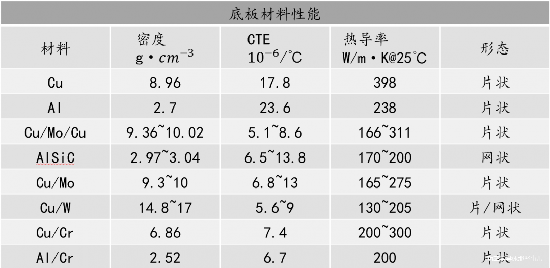
Considering the impact of chemical reactions, all materials will have a nickel layer plated on their surfaces, ensuring good solder wetting, low water absorption, and resistance to corrosion from processing solvents.
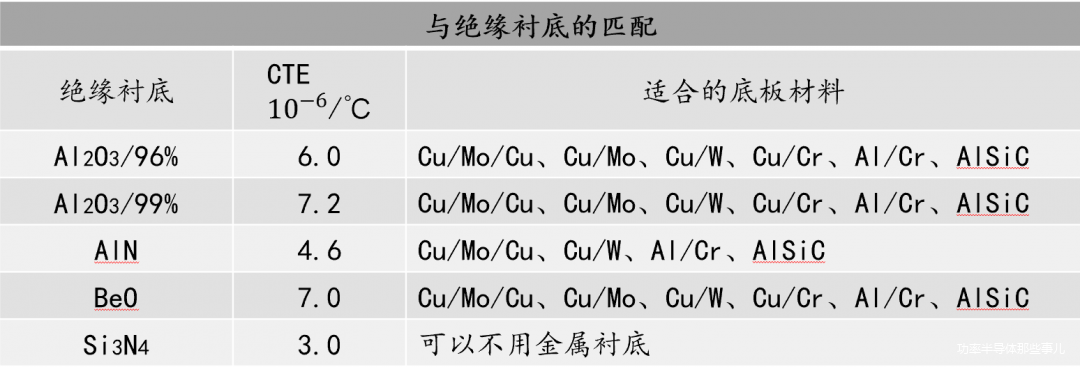
Some Disadvantages of Various Base Plates:
Cu/Mo: High cost, high density, difficult to machine, potential for delamination;
Cu/Mo: High cost, high density, difficult to machine;
Cu/W: High cost, high density
AlSiC Composite Materials
Silicon carbide aluminum composite materials are sheet-like or near-net-shaped materials, currently the most common base plate material aside from copper base plates. Near-net forming processes can deform the thermal conductive sheet’s bottom surface, increasing the thermal conduction area between the base plate and the cooling liquid, facilitating heat dissipation, and reducing processing requirements in mass production.
The manufacturing steps for most near-net forming composite materials are roughly as follows:
① Processing Preparation: Porous silicon carbide particles are injection molded to obtain porous AlC semi-finished products, which can have the geometric features required for the base plate, including cavities, holes, and surface textures. If the pre-treatment temperature is appropriate, manufacturing can also occur on the insulating substrate.
② Penetration: The porous semi-finished product is inserted into a mold of the same size as the finished base plate, and under vacuum and high-pressure conditions, molten refractory aluminum penetrates into the porous semi-finished product, forming various aluminum-silicon alloys to achieve the desired performance.
③ Subsequent Processing: A copper layer is flame-sprayed onto the top of the base plate to enhance the welding capability with the insulating substrate.
Thus, the disadvantages of AlSiC are the difficulty of machining and the strict process control.
As material technology continues to develop, composite materials doped with graphite fibers will have good prospects in high power device applications, while also depending on the future development speed of power modules. Otherwise, even if the development of graphite fiber composite materials is rapid, they will not be applied in power modules. Therefore, we hope to see more power modules with new materials in the near future.
References can be found in the detailed document.
Feel free to scan the QR code to add the editor on WeChat.

Scan to join the knowledge circle and receive public account materials.