From 2000 to 2010, the Chinese semiconductor industry sat on the sidelines for a decade. Before 2014, the golden age of the internet was a winter for semiconductors.A decade is a cycle, and the financing of China’s semiconductor industry has reached a trillion yuan level, with visible bubbles behind the prosperity.Moreover, the international situation is changing dramatically, and geopolitical issues are becoming increasingly prominent, with “bottleneck” problems becoming more pronounced.From “winter” to “winter,” in the past decade, China’s chip semiconductor industry has experienced a complete cycle. As the cold winter approaches again, how to navigate through the cycle has become a key proposition.
(Main Text)
01The Turbulent Domestic and International Chip Industry
The global chip landscape is undergoing unprecedented changes.
The signing of the U.S. “CHIPS and Science Act” has escalated the open and covert struggles within the semiconductor industry chain, with countries and regions such as South Korea and the European Union accelerating the establishment of their semiconductor barriers.The U.S. “CHIPS and Science Act” clearly states that it will provide $52.7 billion in subsidies for semiconductor R&D, manufacturing, and workforce development in the U.S., while restricting related companies from increasing production of advanced process chips below 28nm in China for the next ten years.
In February, the EU announced an additional investment of 15 billion euros in the chip industry to increase chip production capacity and reduce dependence on chip imports from Asia;in early August, South Korea officially implemented the “National Advanced Strategic Industry Act” to strengthen support for the semiconductor industry, while companies like Samsung and SK Hynix pledged to invest 340 trillion won (approximately $260 billion) in South Korea.
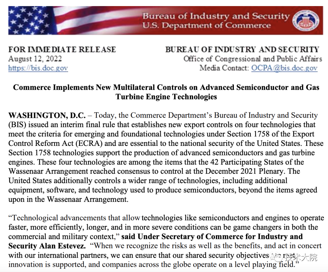
On August 12, the U.S. Department of Commerce’s Bureau of Industry and Security (BIS) published a temporary final rule in the Federal Register, adding four “emerging and foundational technologies” to the export control list, three of which involve semiconductors, including the most upstream and high-end industry EDA in chip design.
These four technologies are among the projects that 42 participating countries reached a consensus to control at a meeting in December 2021, specifically including:
-
Two types of wide bandgap semiconductor materials: Gallium Oxide (Ga2O3) and Diamond
-
Advanced chip EDA software tools for designing GAAFET architecture (Gate-All-Around Field Effect Transistor)
-
Pressure gain combustion technology for gas turbine engines
Among these four technologies, the most attention from the outside world is on EDA software.EDA is the cornerstone industry of electronic design, also known in the industry as the “mother of chips.”
The U.S. Department of Commerce stated that the four emerging and foundational technologies being controlled will “significantly increase military potential”. Being included on this list means that the export of these four technologies will require an export license from the U.S. Department of Commerce.If a company applies for an export license but the U.S. government does not allow it, the aforementioned technologies may not be supplied in the global industry chain.
The global semiconductor investment landscape is changing, and mainland China is also unsettled. Refer to my previous article: The Great Earthquake in the Semiconductor Industry.
In the past decade, China’s semiconductor industry has made significant progress, from the investment germination around 2010, to gradual warming in 2014, and then to rapid prosperity after 2019.Now, with the arrival of the “cold wave,” it will enter a new stage of adjustment and transformation.
As the global situation changes dramatically and geopolitical issues become increasingly prominent, how the semiconductor industry breaks through has become a question that many industry players must consider.
I believe two key points must be grasped:achieving breakthroughs in IP architecture and chip manufacturing processes.
First: Chip design is at the very top of the semiconductor industry, the most core foundation of the semiconductor industry, with extremely high technical barriers.The concentrated embodiment of semiconductor intellectual property is the independent intellectual property IP core (Intellectual Property Core). The open-source RISC-V brings more imaginative space to China’s chip industry,and RISC-V-based processor IP will shine brightly.
Second:The U.S. push for “decoupling and breaking chains” in chips has directly led to restrictions on key nodes in domestic chip processes,and Chiplet technology may become the key to breakthroughs in chip performance.In the future, opportunities in the semiconductor industry will mainly focus on new structures and packaging technologies centered around Chiplet, as well as upstream semiconductor equipment and materials in the industry chain.
02RISC-V IP Architecture Rises Uniquely
What is IP?
IP is a verified, reusable functional module that gradually separates from the chip design process. By using IP cores, designers do not need to start from scratch to redesign all details but can quickly complete the design of a module by adjusting specific IP cores,thus shortening the development cycle, reducing design costs, minimizing the risk of design errors, and improving chip design efficiency.
If we open a chip, we can see that many IPs make up the entire circuit on the layout.These integrated circuit IP cores can be seen and touched in chip design, can perform certain functions, and more importantly, can be reused through licensing to different customers.If we make an analogy, IP is like the “LEGO” modules that make up chip design.
When we want to design a microprocessor chip, we need to first determine which instruction architecture to use, then design the chip and microprocessor based on the instruction architecture, and finally produce the wafer.
There are three different modes of chip design:
-
Closed Design. The Intel X86 system architecture is led by its own company
-
Other companies that need to use its instruction set to design microprocessors must pay for patent licensing
-
From system architecture to chip manufacturing,Intel maintains it all,which belongs to a completely closed design
-
Patent Design. Arm sells patents, not chips
-
Arm provides microprocessor designs and licenses IP to companies like Qualcomm, Apple, and Huawei, which then design their own chips based on the ARM instruction set
-
Some companies use ARM-designed IP to produce their own SoCs or contract chip production
-
Open Design. The open-source RISC-V belongs to this model
-
Anyone can use this instruction set, design based on RISC-V, and then sell the patents; SiFive operates in this model
-
Other companies, such as Western Digital, are developing chips based on the RISC-V open-source instruction set and then processing production
The PC era was dominated by closed design models, while the mobile phone era saw the patent model prevail. Now,RISC-V has pioneered a new open design model.
The 1980s was the most exciting and intense era of chip competition, with the flourishing development of various computer chip architectures.In the decades of processor development, various processor architectures have emerged and flourished. However, after nearly 30 years of industry evolution, other processor architectures have gradually been forgotten in history, leaving only the two dominant architectures: X86 and ARM.
The world has long suffered under ARM’s dominance, and as the once-divided landscape of mobile, desktop, and server markets is about to become ARM’s monopoly, more companies are considering RISC-V, which is significant for RISC-V. This isan excellent opportunity to promote architectural diversityafter the loss of diversity in chip architectures since the 1980s.
Since its inception, RISC-V has attracted significant attention from the industry.Unlike the proprietary instruction set architectures monopolized by foreign commercial companies like x86 and ARM, the biggest feature of RISC-V is its “open standardization“, which is a complete first in the CPU field and an excellent opportunity for a technological revolution in CPU technology.
Mark Himelstein, CTO of RISC-V, said:RISC-V is an open hardware, open-source hardware instruction set architecture:
-
RISC-V is completely open-source, and anyone can use it for free
-
The RISC-V architecture itself is open-source, but the CPU IP cores developed based on the RISC-V architecture are chargeable
-
Similar to open-source Linux and commercial Redhat Linux,commercial RISC-V IP cores can provide better stability, continuity of development, and after-sales service than open-source cores
-
A reduced instruction set computer (RISC) architecture
-
Only 47 instructions
-
In contrast, Arm has over 200 instructions
-
AMD and Intel use complex instruction set computer (CISC) architectures with far more than 1500 instructions
-
Scalability
-
Modular design, only configuring the necessary parts with strict compatibility requirements
-
Engineers can add their own instruction sets
-
Can be used for DSA (Domain-Specific Acceleration)
From a competitive perspective, the Arm architecture and x86 architecture have monopolized the mobile terminal, PC, and server markets for many years, and it will take time for new players like RISC-V to penetrate these fields. However, in emerging fields such as AIoT, new energy vehicle electronics, and heterogeneous computing, RISC-V and other architectures are starting from the same starting line, giving them new advantages that giants do not possess.
Currently,market consolidation, geopolitical priorities, andthe surge of IoT terminalsare driving RISC-V to be adopted more widely. Recently, Callista Redmond, CEO of the RISC-V International Foundation, stated that it is estimated that there are already 10 billion RISC-V cores in the market. Since its birth in 2010, RISC-V has achieved a shipment of 10 billion cores in about 12 years, demonstrating the vitality of this new architecture.
03The Window of Opportunity for RISC-V in China
Given that geopolitical or trade tensions between countries may adversely affect a nation’s technological sovereignty, the EU and China are looking to promote computing technology sovereignty through RISC-V.
In Europe, RISC-V has gained tremendous momentum under the promotion of the European Processor Initiative (EPI):
-
The Barcelona Supercomputing Center is leading the eProcessor project, aiming to build high-performance out-of-order RISC-V ISA processors for HPC use cases
-
In 2020, EPI built a 4096-core RISC-V small chip prototype called Manticore for efficient floating-point computation. Compared to other commercial CPUs and GPUs, this processor’s energy efficiency for floating-point intensive business loads is five times that of the former
In Russia, server manufacturer Yadro, chip design company Syntacore, and technology investment company Rostec have reached a cooperation to build a new CPU based on RISC-V,with a product roadmap that includes a 12nm SoC with four RISC-V cores (clock frequency of 1.5GHz).
In North America:
-
SiFive, founded by the inventors of RISC-V, is headquartered in San Francisco and has received investments from Intel Capital, Qualcomm Ventures, and Western Digital
-
RISC-V cores have already been adopted in storage controllers from Western Digital and Seagate
-
Google is utilizing RISC-V in its OpenTitan project, aiming to enhance computing security through silicon chip roots of trust (RoT) and defend against security threats like Spectre and Meltdown
-
AI CPU startup Tenstorrent announced that its SoC will use SiFive’s 64-bit RISC-V core X280,which integrates a 512-bit wide RISC-V vector extension (RVV)
-
Intel announced a partnership with SiFive, a provider of RISC-V processor cores (for CPUs and coprocessors), to useSiFive’s highest-performance RISC-V processor core P550
In the Asia-Pacific region, China is leading the development of RISC-V technology:
-
Chinese CPU supplier Loongson Technology is developing high-performance CPUs based on RISC-V for HPC
-
Huawei’s HiSilicon has self-developed a main processing chip for analog television (ATV) that supports various global standards, with an inbuilt self-developed 32-bit RISC-V CPU
-
The Chinese Academy of Sciences’ RISC-V “Xiangshan” processor has been taped out and showcased at the RISC-V Summit in San Francisco
-
SiFive China was established in August 2018, with technology sourced from the U.S. SiFive company, focusing on RISC-V CPU IP licensing and chip design
-
ChipRise Technology was founded in June 2018, with a team from leading semiconductor chip design companies, as an independent third-party RISC-V architecture CPU IP licensing company
-
Pingtouge Semiconductor was established in October 2018, originally from Zhongtian Microelectronics, later acquired by Alibaba Group. The company focuses on RISC-V CPU IP licensing and chip design, with the latter as its main business
-
Chipone Technology, based in Hsinchu, Taiwan, was founded in 2005, focusing on RISC-V architecture CPU IP core licensing
In terms of software ecosystem, the RISC-V ecosystem is also rapidly developing, from various mainstream programming languages (such as C, C++, Golang), to mainstream GCC, LLVM, and other compilation systems, to Linux and various RTOS operating system kernels, to common operating system distributions like Ubuntu and Debian, as well as application software like Docker containers, etc.
Currently, except for various algorithm library optimization support, the Android ecosystem, and the server ecosystem where RISC-V is still relatively weak, the rest of the software ecosystem can basically meet the needs of application development. RISC-V has taken about five years to complete the software ecosystem that ARM accumulated over twenty years (1990 – 2010), and even the once-famous CPU manufacturer MIPS has announced its abandonment of the MIPS architecture in favor of the flourishing RISC-V architecture.
China is also investing heavily in building the software ecosystem for RISC-V processors, with the Software Research Institute of the Chinese Academy of Sciences announcing its focus on porting and optimizing Linux distributions for RISC-V processors. It is important to note thatthe window of opportunity that RISC-V offers to China is not long, and we should concentrate our efforts to accelerate the development of RISC-V enterprises.04Chiplet: A Solution for the Post-Moore Era
For a long time, the improvement of chip computing power and efficiency has been achieved under the guidance of Moore’s Law by simply throwing money at it. However, as the efficiency of Moore’s Law declines, the costs associated with chip computing power and efficiency are starting to rise rapidly.
On one hand, with the development of advanced processes, the design costs and complexity of chips have significantly increased; on the other hand, as the entire society becomes more digital and intelligent, the demands for big data, consumer electronics, and autonomous driving are becoming increasingly diverse, and the innovation cycle of chips is constantly being compressed, leading to a significant increase in market demand for customized chips.In the context of continuous upgrades of advanced processes and the increasing difficulty of sustaining Moore’s Law, Chiplet is like a “timely rain”.
Compared to conventional processes, Chiplet mainly brings two changes:
- One is to solve the problem of memory bandwidth not keeping up with processor speed improvements, known as the “memory wall” problem
- The other is to improve yield. Based on wafer-level advanced packaging, the wiring density is short, and there is significant room for improvement in signal transmission rates, which can greatly enhance interconnect density
In summary:split large SoC chips into multiple smaller chips, or even chiplets, and then use advanced packaging technology to connect them together.What is Chiplet technology?
Chiplet, commonly known as a chiplet, is a small chip group that integrates multiple module chips with specific functions through die-to-die internal interconnection technology, forming a system chip. The emergence of Chiplet technology delays the failure of Moore’s Law and slows down the process time, making it an ideal solution for upgrading chip performance in the post-Moore era.
Chiplet is an important way to improve integration and chip computing power in the post-Moore era
Currently, the mainstream technology on the market is SoC, which integrates multiple circuit blocks responsible for different functions onto the same chip die through photolithography, mainly integrating CPU, GPU, DSP, ISP, and other functional computing units and many interface IPs, with a high dependence on advanced nanotechnology.
Compared to SoC,the core advantage of Chiplet lies in cost, including manufacturing costs and design costs:
-
First, under the enormous demand for computing power, the number of transistors in chips has skyrocketed, and the chip area has continuously expanded. Chiplet design divides large chips into smaller chips, effectively improving yield and reducing cost increases caused by defective rates
-
Second, the logic computing units of SoC chips rely on advanced processes to improve performance, while other parts can usually use more cost-effective mature processes. After the Chipletization of SoC chips, different chiplets can be manufactured separately using suitable process nodes as needed, and then assembled through advanced packaging technology, effectively reducing manufacturing costs
Chiplet technology is an important way to continuously improve integration and chip computing power as SoC integration develops into the post-Moore era. Compared to traditional SoC, Chiplet has significant advantages in power consumption, time to market, and cost, effectively addressing the limitations brought by the physical limits of nanotechnology.
05Chiplet Leads New Opportunities in the Packaging Industry
In recent years, the improvement of chip performance has mainly been at the chip level. To address the issues encountered by advanced processes, the industry hopes to shift from the traditional method of solely relying on shrinking transistor feature sizes to improve integration to a system-level design with relatively controllable costs, achieving system-level performance comparable to continued shrinking of transistor feature sizes. This is the essence of Chiplet, 2.5D/3D advanced packaging, and other technologies.
The representative figure advocating Chiplet and advanced packaging is TSMC’s former COO, Zhang Shangyi, known as “Uncle Jiang”; while the current co-CEO of SMIC, Liang Mengsong, advocates advanced processes.
Zhang Shangyi explained in his “ten-thousand-word autobiography” why he is optimistic about advanced packaging: “The graphics chip giant NVIDIA is our customer. They previously had a GPU paired with 8 DRAMs.You need to send many signals back and forth between the GPU and DRAM.If you look at the distance between this GPU and DRAM, it is so far apart.Why are they so far apart? Because the metal lines are very wide.If they are too close, you cannot connect all these metal lines.Because of this, people are willing to pay about 30% of the speed and about 60% of the power consumption to drive these lines.” Zhang Shangyi cited as an example.He also stated that if a silicon wafer replaces a PCB, the GPU and DRAM can be placed side by side, making their performance very similar to being on the same silicon chip.
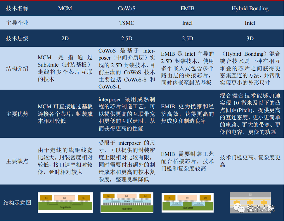
Diversity in functionality, connectivity, and stacking is the development direction of advanced packaging, with connection and extension technologies such as Bumping, TSV, RDL, and Interposer as support, while packaging forms evolve towards 2.5D/3D, multi-die/hybrid integration, which is an important support for realizing Chiplet.
In March 2022, the Chiplet high-speed interconnect standard—UCLE (Universal Chiplet Interconnect Express) was officially launched.This standard aims to establish a global unified interconnection standard at the chip packaging level, thereby creating an open Chiplet ecosystem to jointly implement Chiplet standardization.
UCLE will set various advanced packaging technologies for Chiplet, including the 2.5D packaging technologies led by Intel’s EMIB and TSMC’s CoWoS.As of now, many domestic manufacturers, including Chipone Technology, Moore Elite, ChipMotion Technology, and Alibaba, have successively joined the UCLE alliance, directly benefiting from the relevant technology standards.With domestic manufacturers actively integrating into the UCLE ecosystem, new breakthroughs in Chiplet technology are expected.
Currently, the packaging solutions applicable to Chiplet are mainly SIP, 2.5D, and 3D packaging.2.5D is more like a two-layer small house, while 3D resembles a high-rise building, with higher space utilization efficiency.
-
2.5D packaging technology has developed very maturely and is widely used in FPGA, CPU, GPU, and other chips
-
3D packaging technology is more challenging, currently mastered and commercialized by Intel and TSMC
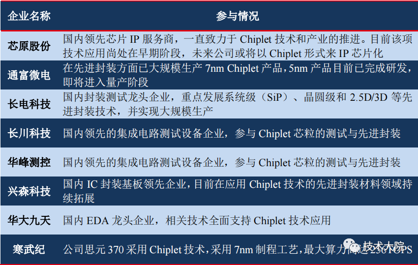
For the industry chain, the current implementation of 2.5D Chiplet mainly benefits packaging companies:
-
For example, Tongfu Microelectronics (002156.SZ), which previously packaged for AMD, has seen its value double compared to traditional packaging, with higher gross margins
-
Secondly, substrate companies, such as Xingsen Technology (002436.SZ), currently have larger chip areas and higher on-chip communication requirements for 2.5D Chiplet processes, increasing the demand for the number of layers and area of substrates, and Xingsen’s ABF substrate production line is expected to receive significant order support
-
Then there are packaging and testing equipment companies, such as Huafeng Measurement and Control (688200.SH), etc.
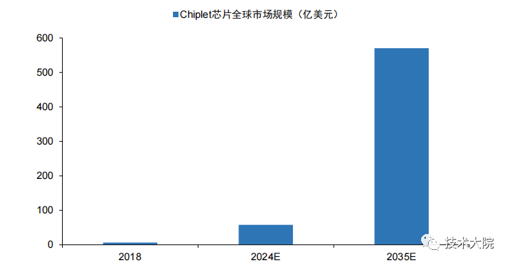
With continuous breakthroughs in underlying packaging technology, it is expected that by 2035, the global Chiplet chip market size will reach $57 billion. Currently, the underlying packaging technology supporting Chiplet has gradually evolved from 2D technology to 3D technology, with significant improvements in economic benefits and overall performance.
According to Omdia data, the global Chiplet chip market size is expected to reach $5.8 billion in 2024, and by 2035, the global market size is expected to exceed $57 billion.Referring to $645 million in 2018, the CAGR from 2018 to 2035 is as high as 30.16%.
In the context of the slowing “Moore’s Law”,Chiplet technology is expected to become the main reliance of chip manufacturers for a considerable period in the future, and as the underlying packaging technology supporting Chiplet continues to break through and become widespread, it will further support its future growth.
06Conclusion
Regarding IP architecture:
Although RISC-V has made significant progress under the promotion of multiple manufacturers,historically,the popularization of any architecture takes time.
For example, the x86 architecture dominated the instruction set architecture market for decades during the PC era, and only after the PC era did the Arm architecture rise, which also took decades to reach its peak.In other words, the transition of computing loads requires a long lifecycle. This means that although we have now entered the era of the Internet of Everything, creating opportunities for RISC-V, this emerging instruction set has only taken its first step.
Regarding Chiplet technology:
For Chiplet, there is a key point that cannot be ignored, which is that its emergence stems from the bottlenecks encountered in advanced processes.Rather than blindly exploring new processes and materials at any cost, Chiplet opens up a new idea that not only reduces the development costs of chips but also better controls yield.
Chiplet consists of multiple heterogeneous integrations, with each chip only needing to use the most suitable process node, rather than all chips using the most advanced process node, which can more effectively utilize existing wafer fabrication lines domestically, reducing the resistance brought by the blockade of advanced process nodes, providing a very good opportunity for the domestic semiconductor industry to break through.Chiplet is a direction, not a specific technology; it can use various packaging technologies to achieve this. For the domestic semiconductor industry,the greatest significance of Chiplet in the context of limited advanced process development is to exchange time for space. For China, the benefits of developing Chiplet are numerous. Logically, it seeks to balance performance, manufacturing costs, and time costs.I firmly believe that with the promotion of RISC-V architecture IP and breakthroughs in Chiplet technology, China’s chips will usher in a golden decade of development, surely finding their own path to breakthrough. (End of Text)