In the second week of June, China’s semiconductor industry welcomed a timely policy “rain”.
From Zhuhai High-tech Zone launching ten special support measures, to Guangzhou Huangpu District issuing nine new policies for integrated circuits, and to Shanghai Mayor Gong Zheng emphasizing in the “Learning Times” that “the development of the entire integrated circuit chain should be driven by production lines”, the three cities have successively rolled out a series of policy initiatives within six days.
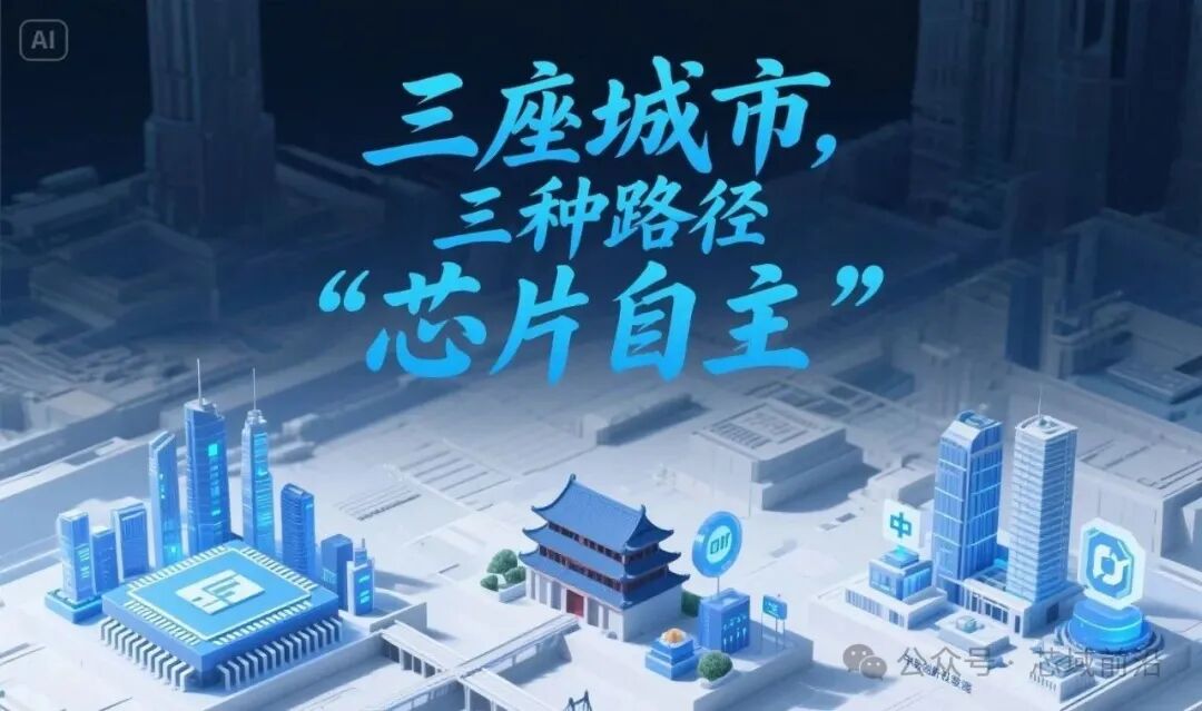
These policies all point to the same goal: to build a self-controllable semiconductor industry chain.
Zhuhai focuses on RISC-V ecosystem construction, Guangzhou aims for breakthroughs in high-end chip design, and Shanghai is pushing for third-generation semiconductor materials, forming a complementary policy landscape that weaves a large net for China’s semiconductor industry to break through.
01
—
Intensive Policy Period: The “Chip” Actions of Three Cities in Six Days纳
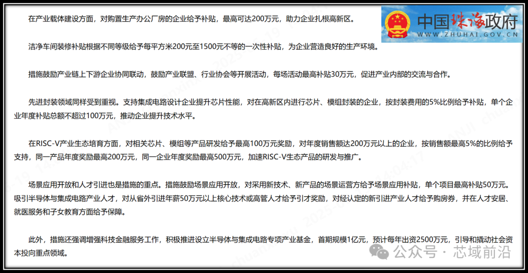
On June 12, Zhuhai High-tech Zone took the lead by proposing “ten measures” to provide substantial financial support for semiconductor and integrated circuit companies in key areas such as factory purchase, workshop decoration, industry chain collaboration, and advanced packaging.
The most notable aspect is the special cultivation of the RISC-V (based on the fifth generation of reduced instruction set) ecosystem.
According to the policy, RISC-V chip products listed in Zhuhai’s innovation product list will receive a reward of up to 1 million yuan;
For companies with annual sales of a single chip exceeding 2 million yuan, a reward of up to 5% of sales will be given, with a maximum annual reward of 5 million yuan for a single company.
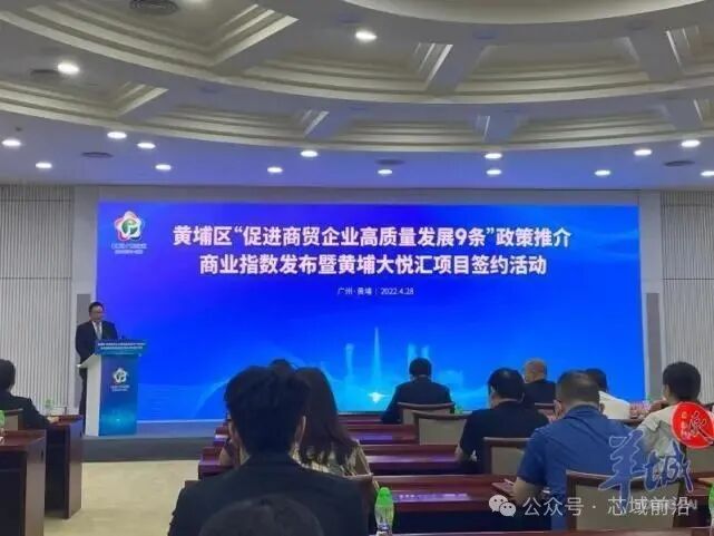
Just four days later, on June 16, Guangzhou Huangpu District followed up with nine special policies aimed at creating a “core bearing area for China’s integrated circuit industry third pole”.
This district directly targets the enhancement of high-end chip design capabilities, focusing on the development and design of CPUs (central processing units), GPUs (graphics processing units), and FPGAs (field-programmable gate arrays).
Notably, the Guangzhou policy particularly emphasizes the localization of core tools.
For enterprises purchasing domestic EDA (electronic design automation) tools and IP (intellectual property) licenses, a subsidy of up to 30% of the actual purchase amount will be provided.
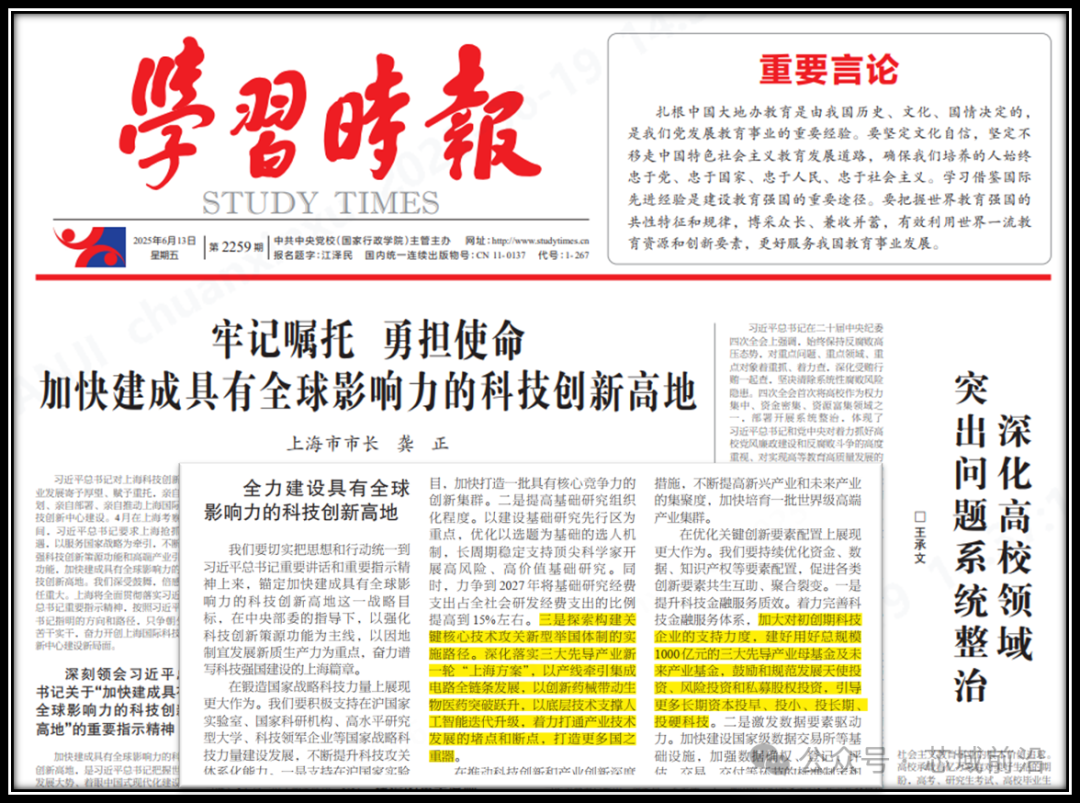
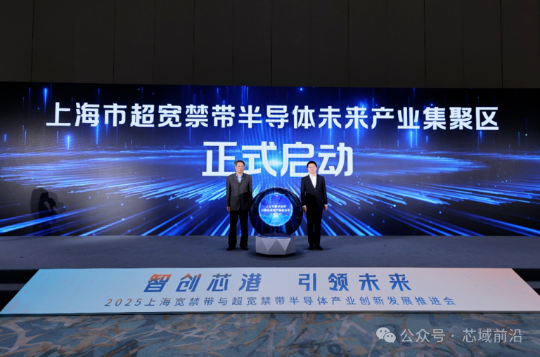
Meanwhile, on June 13, Shanghai Mayor Gong Zheng announced through the “Learning Times” that Shanghai will “deepen the implementation of a new round of ‘Shanghai Plan’ for the three leading industries”, particularly emphasizing the need to “drive the development of the entire integrated circuit chain with production lines”.
Shanghai also clearly stated the need to “build and utilize a mother fund for the three leading industries with a total scale of 100 billion yuan”, which includes two integrated circuit funds in the second batch of sub-funds.
This series of actions, densely implemented within six days, reflects the urgency of China’s semiconductor industry for independence.
02
—
Distinctive Features of the Three Cities: Differentiated Layouts Constructing a Complete Picture
Upon careful analysis of the policies from the three regions, it is evident that they each have their own focus in supporting the development of the semiconductor industry, forming a complementary pattern.
Zhuhai’s Ambition for RISC-V
Zhuhai has made the construction of the RISC-V ecosystem a key focus for breakthrough.
Among the ten measures, the seventh measure specifically establishes “vigorous cultivation of the RISC-V industrial ecosystem”, which is quite rare in local policies.
This layout has been well-prepared.
In 2024, Zhuhai established the world’s first RISC-V-based industrial innovation cooperation organization—the RDSA Industrial Alliance;
In May of this year, the Zhuhai RISC-V Ecological Application Innovation Center was also inaugurated in the high-tech zone.
Local enterprises have already begun to reap the benefits.
LeapFrog Technology, established just five years ago, completed over 200 million yuan in Series B financing in May, led by the Zhuhai New Quality Productivity Investment Fund.
The company has launched multiple SoC (system on chip) chips based on the RISC-V architecture, with cumulative sales reaching millions of units.
Guangzhou’s Full Industry Chain Layout
Guangzhou Huangpu District demonstrates ambition in constructing a complete industry chain.
The policy clearly aims to break through in five key areas: chip design, specialty processes, packaging and testing, EDA tools, and equipment and components.
Currently, the district has gathered over 150 integrated circuit companies, accounting for nearly 90% of Guangzhou, forming a complete industry chain from design to manufacturing, packaging, testing, and equipment materials.
Guangzhou’s policy particularly emphasizes “strengthening and supplementing the chain”.
On one hand, it encourages the development of high-end semiconductor materials such as photomasks, electronic gases, and photoresists; on the other hand, it supports the localization of equipment and key components for photolithography, cleaning, and etching.
The leading enterprise in the district, Yuexin Semiconductor, submitted its IPO guidance filing in April this year, expected to become “Guangzhou’s first chip”.
Shanghai’s Leadership in Third-Generation Semiconductors
As a major hub for China’s semiconductor industry, Shanghai’s integrated circuit industry scale is expected to exceed 390 billion yuan in 2024, with a year-on-year growth of over 20%, maintaining its position as the national leader.
The focus of its policy is on seizing the technological high ground—wide bandgap and ultra-wide bandgap semiconductor (third-generation semiconductor) materials.
On May 12, the ultra-wide bandgap semiconductor future industry cluster in Shanghai’s Lingang New Area began construction, and ten special support policies were released.
This area focuses on silicon carbide (SiC) and gallium nitride (GaN) materials, creating a complete industry chain from R&D to application.
Wu Xiaohua, deputy secretary of the Lingang New Area Party Working Committee, stated that Lingang plans to achieve a “double hundred billion” goal by 2026: equipment materials and wafer manufacturing scale exceeding 10 billion yuan, and module device scale exceeding 10 billion yuan.
03
—
Behind the Policies: Three Strategic Paths for Self-Control
Although the policies of the three regions have local characteristics, they are highly consistent in strategic paths, all pointing to the core goal of “self-control”.
Path One: Breaking Through Core Tool Bottlenecks
EDA tools and IP cores are the “throat” of chip design, long monopolized by foreign giants. The policies of the three regions all prioritize breaking through this bottleneck.
Zhuhai’s support for EDA is arguably the highest in the country:
-
30% subsidy for enterprises purchasing EDA tools (up to 3 million yuan annually);
-
50% subsidy for renting EDA tools (up to 1 million yuan annually);
-
Annual subsidies of up to 10 million yuan for enterprises developing EDA and achieving industrialization.
Guangzhou focuses on promoting the application of domestic EDA, providing a subsidy of up to 30% of the actual purchase amount for enterprises purchasing domestic EDA and IP licenses, with a maximum of 1 million yuan per enterprise annually.
Path Two: Reducing R&D Risk Costs
Chip R&D often requires several million yuan in wafer processing costs, deterring many innovative enterprises. The policies of the three regions all aim to reduce enterprise risks through high subsidies.
Zhuhai’s support for wafer processing is astonishing:
-
70% subsidy for MPW (multi-project wafer) processing (up to 3 million yuan annually);
-
50% subsidy for the first round of full mask processing before mass production of engineering products, with an annual subsidy of up to 8 million yuan for processes using 14nm or below.
Guangzhou provides a maximum of 40% tiered subsidy for design enterprises using MPW processing or completing full mask engineering processing, with a maximum of 5 million yuan per enterprise annually.
Path Three: Building an Industrial Ecosystem
It is difficult for a single enterprise to support the entire industry chain, and the policies of the three regions emphasize ecosystem construction.
Shanghai guides ecological development through a trillion-level industrial fund. In addition to the 100 billion yuan mother fund for the three leading industries, Shanghai has also established a 10 billion yuan integrated circuit design industry merger fund to promote industry consolidation.
Zhuhai actively promotes the establishment of a 100 million yuan special industrial fund for semiconductors and integrated circuits, with an initial investment of 25 million yuan to guide social capital into key areas.
04
—
New Industrial Ecosystem: Innovative Forces Supported by Policies
With policy support, a number of innovative enterprises are rapidly growing, constructing a new ecosystem for China’s semiconductor industry.
The RISC-V ecosystem in Zhuhai is already taking shape.
LeapFrog Technology has completed its layout of edge and endpoint chip products in its five years of establishment, with its RISC-V architecture-based SoC chips covering the fields of AIoT perception, control, and edge computing.
As policies intensify, more enterprises are expected to join this ecosystem.
In Guangzhou, the IPO process of Yuexin Semiconductor marks the maturity of local manufacturing.
This company, established in 2017, is the first 12-inch chip manufacturing enterprise to enter mass production in the Guangdong-Hong Kong-Macao Greater Bay Area, filling a gap in Guangzhou’s manufacturing industry.
Shanghai’s wide bandgap semiconductor industry chain has initially formed.
The Lingang New Area has gathered a number of leading enterprises such as ChipSource Micro, TuoJing Technology, Huahai Qingke, and TianYue Advanced, covering equipment, materials, design, and manufacturing.
Innovation platform construction is also accelerating.
Shanghai recently launched ultra-wide bandgap semiconductor concept verification centers and integrated circuit materials concept verification centers to help projects break through the bottleneck from early technology verification to industrial transformation.
Meanwhile, Zhuhai supports providing public technical services such as chip reliability testing and chip simulation verification, with a maximum subsidy of 5 million yuan.
05
—
The Road Ahead: Challenges from Following to Running Alongside
Despite the intensive rollout of policies, China’s semiconductor industry still faces multiple challenges in achieving a leap from following to running alongside.
The localization of materials and equipment is the biggest shortcoming.
Shanghai’s latest “Implementation Plan for High-Quality Development of the New Materials Industry” frankly states the need to “implement a materials supplement and strengthening project of ‘five chains, multiple categories, and multiple products'”, focusing on breakthroughs in advanced process electronic chemicals, photoresists, polishing materials, etc.
These breakthroughs in basic materials require long-term investment.
Industry consolidation is also urgent.
Bu Rixin, a partner at Chuangdao Investment Consulting, pointed out that after the IPO dividend period for chip design companies ends, “only through mergers and acquisitions, accelerating industry consolidation, can we promote healthy industry development”.
This is precisely the deep meaning behind Shanghai’s establishment of a 10 billion yuan integrated circuit design industry merger fund.
Talent aggregation is another key factor.
Zhuhai’s policy offers a maximum subsidy of 100 million yuan for innovative entrepreneurial teams; for projects selected by Guangdong Province to introduce teams, matching support will be provided at a ratio of 1:1.
This high-intensity investment reflects the current shortage of high-end talent.
According to Semico Research, the RISC-V chip market is expected to exceed 45 billion dollars by 2025, with a compound annual growth rate of 58%.
Whether China can seize the opportunity in this emerging field will be an important test of policy effectiveness.
Next to the wide bandgap semiconductor production line in the Lingang New Area, engineers are debugging newly installed silicon carbide crystal growth furnaces;
In the Zhuhai High-tech Zone RISC-V Innovation Center, young R&D teams are verifying the energy efficiency performance of new architecture chips;
In the cleanroom of Yuexin Semiconductor in Guangzhou Huangpu District, 12-inch wafers are completing micron-level circuit etching under photolithography machines.
Three cities, three paths, all pointing to the same goal—chip independence.
The policy dividends have arrived, the industrial army has moved, and China’s semiconductor industry’s journey towards independence is accelerating into the depths of technology.
 Original Statement: This article is compiled from public information,reproduction requires authorization.If you like it, please give it a“Look”.