In the fields of microelectronics and optoelectronics, the optical properties of semiconductor thin film materials play a decisive role in their practical applications in various devices. The degree of transparency of the materials is closely related to their band structure, electronic behavior characteristics, and microscopic morphology. This article selects silicon-based materials, metals, and metal compounds as research subjects to systematically study the laws of transparency changes and their intrinsic physical mechanisms.
1. Transparent Materials and Their Mechanisms
1. Oxides and Nitrides: Unique Advantages of Wide Bandgap Materials
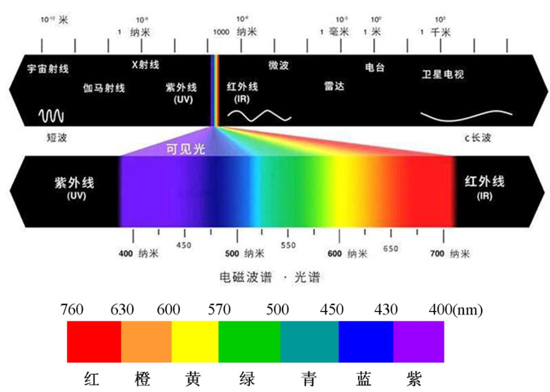
Silicon dioxide (SiO₂) and silicon nitride (Si₃N₄) are representative transparent materials. SiO₂ has a bandgap of up to 9 eV, significantly higher than the energy range of visible light photons (1.6 – 3.1 eV), resulting in minimal absorption of visible light and thus exhibiting high transparency. Si₃N₄ has a bandgap of about 5 eV, which, although slightly lower than that of SiO₂, is still above the energy level of visible light, with a transmittance exceeding 90% in the wavelength range of 400 – 700 nm. Tantalum oxide (TaO) has a bandgap of about 4.4 eV, showing good transparency to visible light but absorbing near-ultraviolet light (wavelength < 280 nm). The transparency of these materials is fundamentally due to their wide band structure, where the energy of photons is insufficient to promote electronic transitions, only causing weak lattice vibration absorption.
2. Characteristics of Amorphous Silicon
Amorphous silicon (a-Si) has a bandgap of about 1.7 eV, which is wider than that of crystalline silicon (1.1 eV), but it can still absorb some visible light (such as blue-green light). Its transparency is closely related to the thickness of the film: when the film thickness is less than 50 nm, the transmittance of red light can reach 40%, making it commonly used in stacked solar cells to achieve selective light transmission functionality.
2. Opaque Materials and Their Mechanisms
1. Silicon-based Semiconductors: The Relationship Between Bandgap and Light Absorption
Both crystalline silicon and polycrystalline silicon have a bandgap of 1.1 eV, corresponding to an absorption edge wavelength of about 1127 nm. High-energy photons in visible light (such as blue light, with an energy of 2.75 eV) can be strongly absorbed, causing the material to appear opaque in the visible light spectrum. Even when the thickness is reduced to 10 nm, the transmittance remains below 30%, primarily due to the high absorption coefficient associated with direct bandgap transitions.
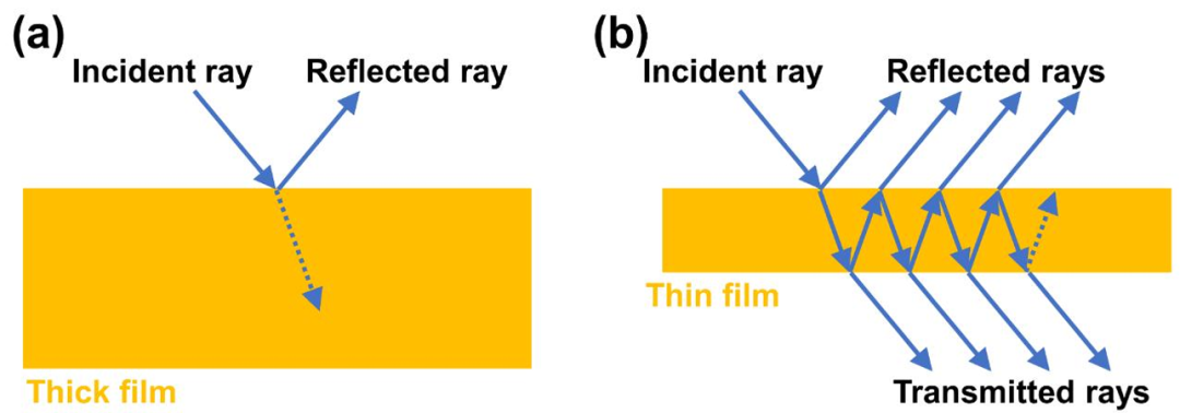
2. Metallic Materials: The Shielding Effect of Free Electrons
Metals such as copper, aluminum, and titanium contain a large number of free electrons, with their plasma frequency in the ultraviolet range (>10¹⁵ Hz). When visible light is incident, the photon energy is lower than the plasma frequency, causing collective oscillation of electrons, resulting in high reflection (>90%) and strong absorption phenomena. For example, a 100 nm thick aluminum film has a reflectance of up to 95% for visible light, while its transmittance is less than 0.1%.
Knowledge Expansion:
The presence of free electrons: Metals like copper, aluminum, and titanium have a large number of freely moving electrons, which are not tightly bound to atoms as in insulators, allowing them to move freely throughout the metal crystal structure. This is a key reason for the good conductivity of metals and is crucial for understanding their optical properties.
Plasma frequency: A large number of free electrons exhibit behavior similar to plasma, resulting in a characteristic frequency known as plasma frequency. The plasma frequency of metals is in the ultraviolet range (greater than 10¹⁵ Hz), meaning that free electrons will only effectively resonate with external electromagnetic fields when the frequency reaches or exceeds this value.
Interaction of visible light with electrons: The frequency of visible light is lower than the plasma frequency of metals. When visible light strikes the surface of a metal, the energy carried by the photons is insufficient to promote free electrons to higher energy levels, but it can cause collective oscillation of free electrons. This oscillation can be imagined as a large number of free electrons moving collectively under the ‘push’ of photons, similar to a school of fish swimming together in response to disturbances in a pond.
High reflection and strong absorption: During the collective oscillation of free electrons, they collide with surrounding metal ions and undergo other interactions, converting the absorbed photon energy into thermal energy, which is the absorption of light by metals; simultaneously, the oscillating electrons re-radiate electromagnetic waves, which manifests as light reflection. Due to this mechanism, metals have a high reflectance for visible light (over 90%) and a very low transmittance (for example, a 100 nm thick aluminum film has a visible light transmittance of less than 0.1%), which is why most metals appear opaque and exhibit a shiny metallic luster.
3. Metal Compounds: The Connection Between Conductivity and Light Absorption
Titanium nitride (TiN) exhibits metallic-like conductivity, and its optical properties are also similar to those of metals. In the visible light region, the imaginary part of the refractive index of TiN is relatively large (k>2), leading to strong light absorption. Experimental data shows that a 50 nm thick TiN film has a transmittance of only 0.5% for light at a wavelength of 550 nm, and it is currently mainly used in photothermal conversion devices.
3. Core Elements of Transparency Regulation
1. Band Engineering and Doping Technology
By doping elements, the bandgap of materials can be adjusted. For example, doping fluorine into SiO₂ can widen the bandgap to 9.5 eV, further reducing absorption of ultraviolet light; doping nitrogen into tantalum oxide (Ta₂O₅) to form TaON can reduce the bandgap to 2.4 eV, allowing partial transmission of visible light.
2. Microstructure Design
Porous structures can reduce the effective refractive index of materials, minimizing reflection losses at interfaces. For instance, porous SiO₂ films (500 nm thick) can achieve a transmittance of 99.6%, nearly reaching the theoretical limit. Nanocrystal/amorphous composite structures (such as nc-Si/a-SiO₂) can utilize quantum confinement effects to regulate the light absorption edge.
3. Ultrafine Processing Technology
When the thickness of metallic films is less than 10 nm, unusual transparency phenomena can occur due to the limitation of the average free path of electrons. For example, a 5 nm thick gold film can achieve a transmittance of 15% in the green light range, which can be used to fabricate transparent electrodes.
4. Research Conclusions
The transparent properties of materials fundamentally depend on the electronic band structure and carrier concentration. Wide bandgap insulators (such as SiO₂, Si₃N₄) and some oxides (Ta₂O₅) exhibit transparency due to the lack of low-energy light absorption pathways; narrow bandgap semiconductors (such as Si) and metallic materials are opaque due to interband absorption or free electron response. In the future, precise control of the band structure and optimization of micro-nano structures are expected to further expand the application range of transparent materials and promote the development of flexible optoelectronic device technology.
The ENDWe welcome everyone to communicate and share daily insights on chip manufacturing. Your attention, likes, and views are my motivation to continue creating high-quality articles. Thank you!We welcome everyone to communicate. Long press the image to add WeChat and join the group chat, noting your name + company + position. Thank you!