When designing PCBs, there are many small details to pay attention to. Let’s see if you are a detail-oriented person.
 1. When calculating the routing length, include the length of the vias and pads that the signal passes through.
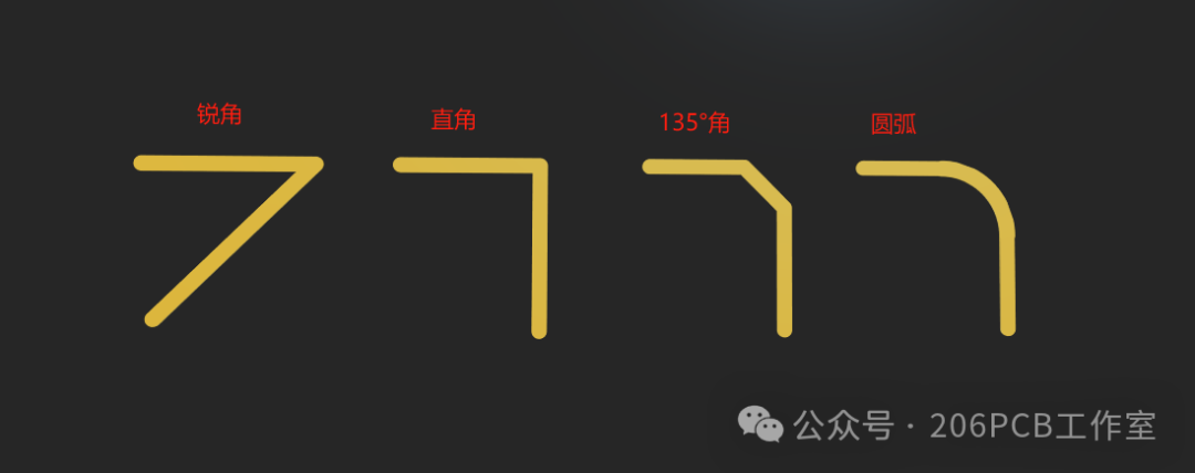
2. During routing, avoid right angles and sharp angles that can cause signal reflections. Preferably use 135° angles; for high-speed and high-frequency signals, use arcs or 10° angles for routing.
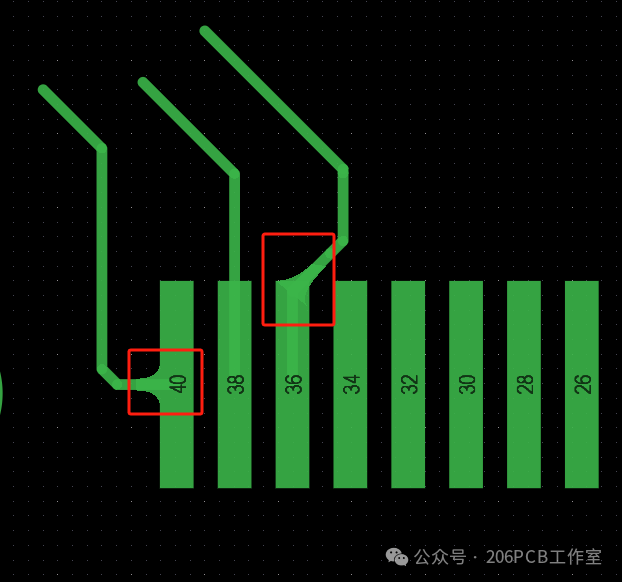
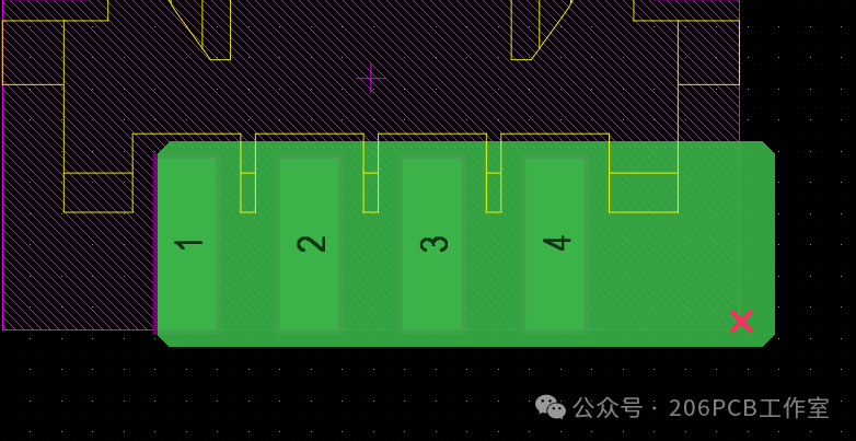
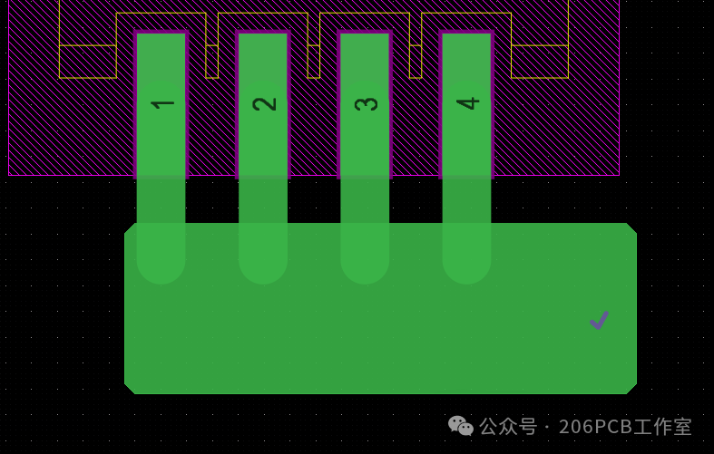
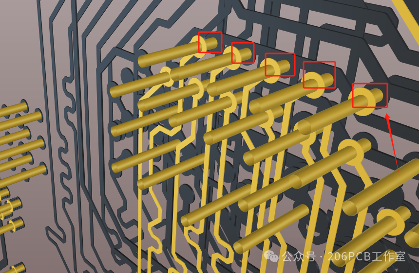
3. When routing from pads, route from the long side of the pad, avoiding routing from the wide side or corners. If unavoidable, try to add a teardrop.
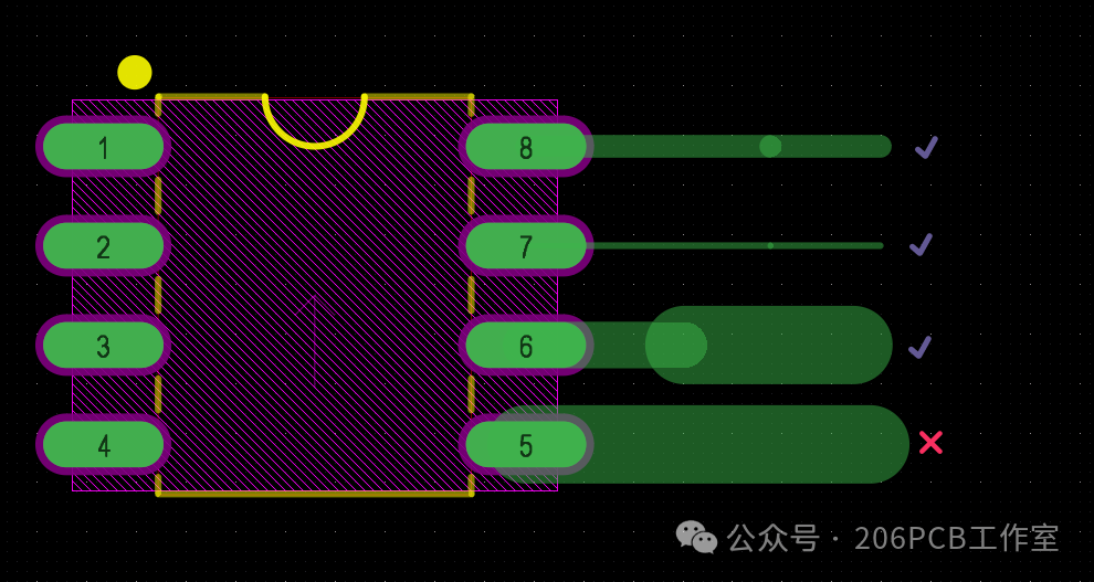
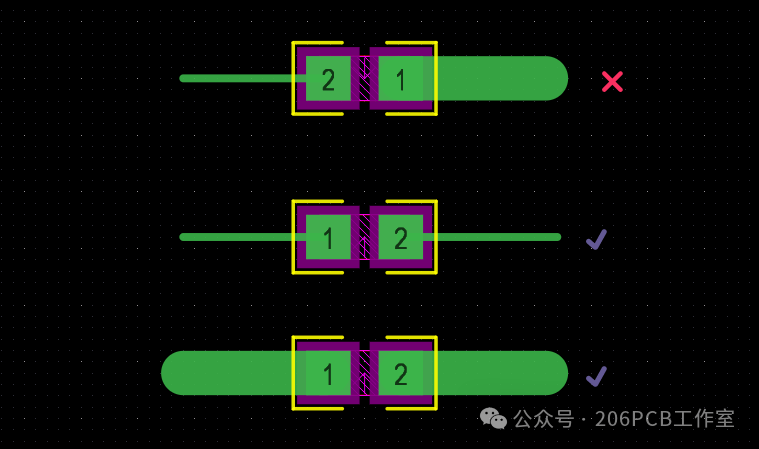
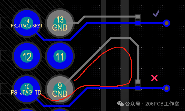
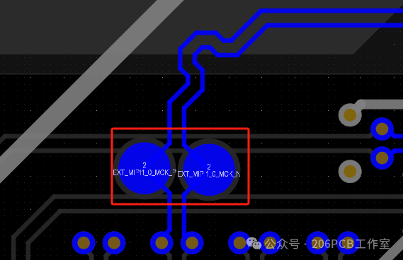
4. When adjacent pads are on the same network, avoid direct connections to reduce the defect rate of the components; it is best to route from the pads before connecting.
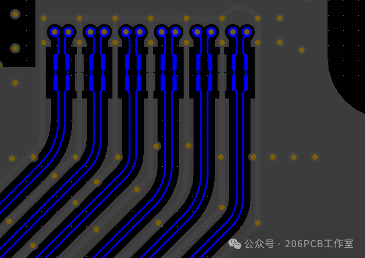
5. For small surface mount devices, pay attention to the symmetry of the routing, maintaining consistent line widths at both ends to reduce the risk of component displacement or tombstoning during reflow.
6. For signals that require ground shielding, ensure to add multiple GND vias along the ground line, keeping the spacing around 50-150 mils to ensure signal integrity. If space does not allow for vias, consider removing ground lines or increasing spacing as alternatives.
7. High-speed signal lines require a complete and continuous reference plane to avoid impedance discontinuities caused by crossing splits.
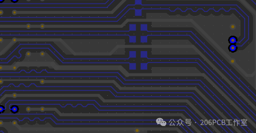
8. Since the pads of surface mount devices can lower impedance, to minimize the impact of impedance discontinuities, consider cutting out the X layer below the pad (X needs to be calculated for impedance, checking how many layers to cut out, or simulating to check signal quality).
9. Signal routing should minimize loop area as much as possible.
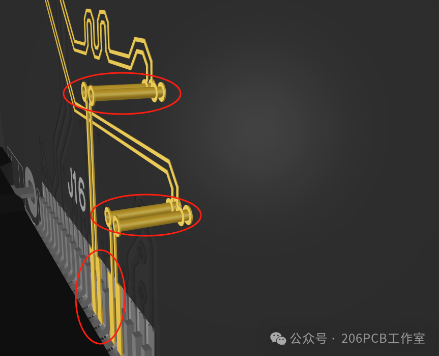
10. Routing should avoid STUBs; for high-speed signals, minimize via STUBs, especially if the remaining length exceeds 12 mils, it is recommended to simulate to assess the impact of via STUBs on signal integrity.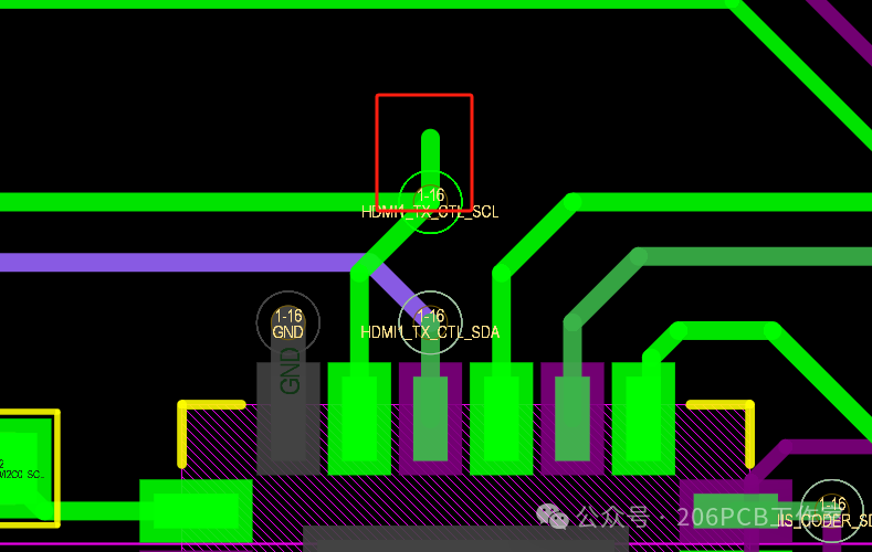
11. Routing should avoid creating closed loops to prevent forming loop antennas, which increases EMI radiation intensity.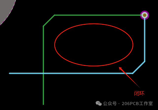 12. It is recommended not to place test points on high-speed signals, as test points can easily cause impedance discontinuities.
13. For modules that may cause interference or are susceptible to interference, consider planning for shielding, with a conventional shield width of 40 mils, and add as many GND vias on the shield as possible to enhance the shielding effect.
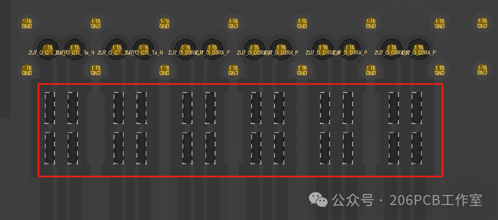
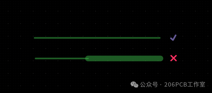
14. During high-speed signal routing, maintain consistent line widths; variations in line width can lead to impedance discontinuities causing signal reflections. In cases where the spacing of BGA fan-out is too small, it is unavoidable for line widths to shrink; efforts should be made to minimize the length of inconsistent line widths.
15. IC pin routing should be less than or equal to the width of the pad; if there are current-carrying requirements, route the line the same width as the pad, then widen it after extending 6-10 mils.