1. What is Measurement/Detection Equipment? What is the Market Landscape?
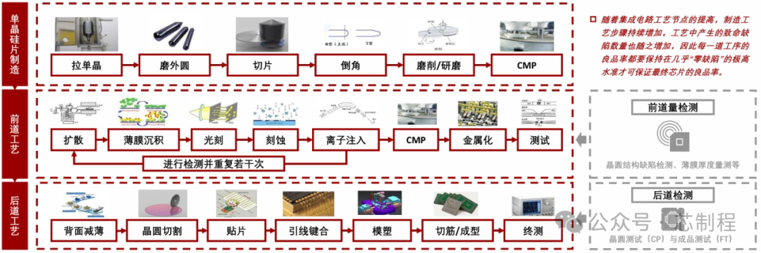
Firstly, measurement/detection is divided into front-end detection and back-end detection. With the advancement of integrated circuit process nodes, the number of manufacturing process steps continues to increase, leading to a rise in the number of critical defects generated during the process. Therefore, the yield rate of each process must be maintained at an extremely high level of nearly “zero defects” to ensure the final yield rate of the chips.
In short:
• Measurement/detection equipment is key to ensuring the yield rate of chip production.
• It is an important link in improving product yield, reducing production costs, and advancing process iterations, and largely determines the competitiveness of foundries.
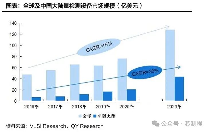
Secondly, in 2023, the global semiconductor measurement/detection equipment market size reached $12.83 billion, a year-on-year increase of 1.6%, with a CAGR of 19.1% from 2019 to 2023. The market size of semiconductor measurement/detection equipment in mainland China grew from $1.69 billion in 2019 to $4.02 billion in 2022. It is predicted that the global semiconductor measurement/detection equipment market will reach $15.9 billion and $19.6 billion in 2024 and 2025, respectively, while the market size in mainland China will be $5.5 billion and $6.8 billion.
According to VLSI data statistics, the CR5 of the global semiconductor measurement/detection equipment industry exceeded 84% in 2023, with major suppliers including KLA, Applied Materials, and Hitachi, among which KLA Semiconductor holds a market share of up to 55.8%.
2. What are the Focus Areas of Measurement/Detection Equipment? Does it Involve “Choke Points”?
Firstly, it is one of the representatives of “choke points”. Since 2022, the US, Japan, and the Netherlands have successively implemented chip export control measures against China. Measurement/detection, as an important type of equipment in the wafer manufacturing process, plays a role comparable to that of the well-known lithography machines, and its role also includes lithography, etching, and packaging processes. It is currently in a golden period for domestic substitution. As core equipment for semiconductor process control, domestic substitution is imperative.
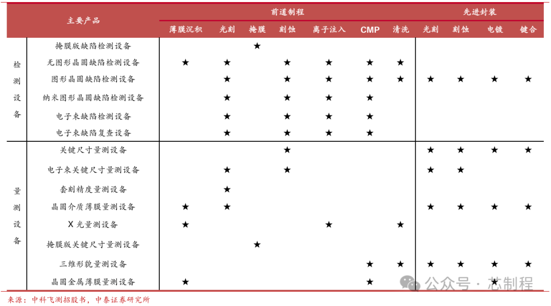
Secondly, Chinese wafer detection equipment manufacturers have products covering both patterned and non-patterned defect detection, electron beam defect detection/re-inspection, and have basically achieved preliminary coverage of processes at 28nm and above. Leading domestic manufacturers are developing or validating products for more advanced process nodes.
However, the harsh reality is that due to the rapid development of advanced technologies and the long-term accumulation of foreign manufacturers, domestic wafer detection equipment manufacturers lag behind overseas manufacturers in the following aspects:
1. The product coverage is not as extensive as that of overseas manufacturers. KLA Semiconductor (KLA) covers almost all front-end detection products, with a coverage rate exceeding 90%. Applied Materials (AMAT) and Onto Innovation also have a front-end detection product coverage rate exceeding 60%, while most domestic manufacturers have a coverage rate of 20%-30% for front-end detection products;
2. The product process nodes are far behind those of leading overseas manufacturers. Currently, domestic wafer detection equipment manufacturers can only mass-produce products for processes of 28nm and above, while products for processes below 28nm are still under development and validation. Leading overseas manufacturers can generally cover processes below 2Xnm, and KLA’s non-patterned wafer defect detection product Surfscan SP7XP has already been applied in processes of 5nm and below.
3. What is the Development Status of Domestic Measurement/Detection Equipment? Who are the Major Players?
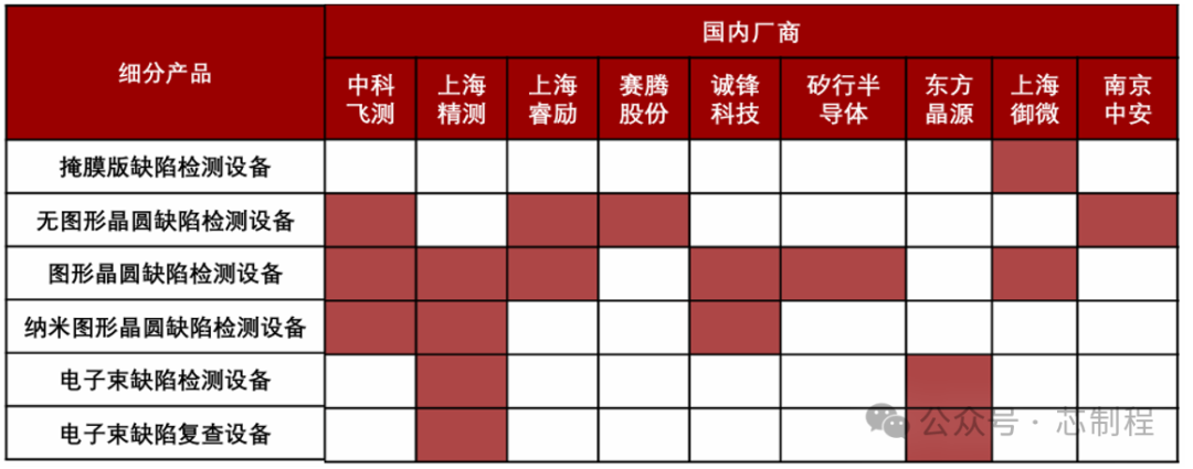
Domestic wafer detection equipment manufacturers include ZK Fly Measurement, Shanghai Jingce, Shanghai Ruile, Saiteng Co., Chengfeng Technology, Xihang Semiconductor, Dongfang Wafer, Shanghai Yuwei, Nanjing Zhong’an, etc.
Chinese wafer detection equipment manufacturers have covered front-end wafer detection equipment such as mask defect detection equipment, non-patterned wafer defect detection equipment, patterned wafer defect detection equipment, nano-patterned wafer defect detection equipment, electron beam defect detection equipment, and electron beam defect re-inspection equipment, and have continuously obtained purchase orders from domestic semiconductor manufacturers, breaking the monopoly of overseas manufacturers.
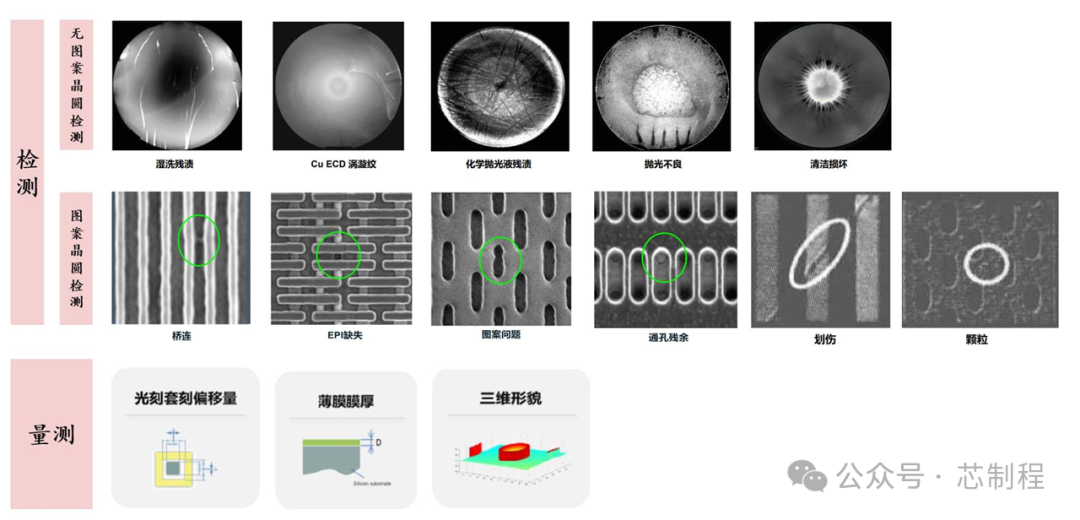
4. What are the Main Functions of Measurement/Detection Equipment? What are the Main Detection Contents?
• Appearance and Cleanliness Inspection: Visual or microscopic observation of bare wafers to detect scratches, particle contamination, defects, and other macroscopic conditions. Non-patterned wafer detection commonly uses dark field microscopy or laser scattering technology, where a laser beam is directed onto a rotating wafer, and scattered light is used to locate surface particles/defects.
• Film Thickness and Material Measurement: After various deposition, annealing, or CMP processes, the thickness and properties of films are measured. Common methods include optical ellipsometry, interferometry, prism coupling, as well as four-point probe and eddy current electrical methods. An ellipsometer can measure changes in polarized light at a certain angle of incidence to directly obtain film thickness and optical constants; the four-point probe and eddy current methods estimate thickness by measuring film resistance or coil impedance.
• Critical Dimension (CD) Measurement: Online measurement of line widths, sidewall angles, etc., formed after photolithography development and etching. Non-imaging optical scattering (OCD) technology is typically used to measure the optical scattering spectrum to invert the three-dimensional morphology of etched trenches/line widths. As process nodes shrink, scattering measurements gradually extend from visible light to deep ultraviolet and even X-ray bands to improve sensitivity.
• Wafer Morphology and Bow/Warp Measurement: Assessment of overall wafer flatness and stress, such as measuring warpage and stress distribution using laser interferometry and other methods.
• Lattice Defect Detection: Lattice defects (point defects, dislocations, stacking faults, etc.) within silicon wafers can be identified using non-destructive techniques such as X-ray diffraction (XRD). XRD reveals internal defects and internal stress distribution through the interaction of X-rays with the crystal structure, requiring no special preparation and can detect dislocations, stacking faults, and other defects within the silicon wafer.
• Metal Contamination Detection: Quantitative detection of trace metal contaminants on wafer surfaces using total reflection X-ray fluorescence (TXRF) and inductively coupled plasma mass spectrometry (ICP-MS) technologies. TXRF excites the wafer surface at a very small angle, detecting only elements within the top 3–8nm range, allowing for sensitive scanning of metals such as Cu and Fe and achieving contamination mapping.
• Defect Re-inspection and Classification: For defects detected by automatic scanning, optical microscopes or scanning electron microscopes (SEM) are used for re-measurement confirmation and detailed classification. SEM can also be used for defect analysis before 3D stacking or wafer backside probe testing.
v
 (Some defect images)