The ground plane and power plane are large conductive areas in PCB design with various purposes. The ground plane provides a common reference point for electrical signals and serves as a return path for current. The power plane transmits power voltage to various components on the circuit board, helping to evenly distribute power across the PCB, thereby reducing voltage drop and ensuring stable power supply. Although the power plane has many advantages, it also requires careful planning of the current return path to prevent signal degradation, especially in mixed-signal designs.
The Importance of Power and Ground Planes
The ground plane helps reduce noise and electromagnetic interference (EMI) by providing a low-impedance path for return currents, thus improving and maintaining signal integrity. When used in conjunction with the power plane, they can also enhance power transmission and help prevent power drop issues in applications with sudden, short-term peaks in power demand. The added solid conductive materials also help dissipate heat generated by components on the PCB, improving thermal management without increasing costs. For designers, the ground and power planes eliminate the need for manual routing, simplifying layout and enabling higher density designs.Conversely, due to the physical characteristics involved in electronic devices, reference planes and power planes can also present some challenges. The proximity of conductive elements and the dielectric materials between them naturally create capacitance between any two adjacent layers in the PCB. This process includes the signal routing layer and the power plane, and if these factors are not considered in PCB design, it may lead to issues.
Return Current Paths in Multilayer PCBs
In pure digital designs with short signal rise times (on the order of a few nanoseconds), return current paths often run closely alongside signal traces. Induced currents in the recent ground plane tend to spread in a narrow Gaussian distribution shape. However, in analog designs, return current paths may not flow directly along the traces. Instead, return currents may span a relatively wide area around the traces that transmit analog signals. In these cases, the lower the switching frequency of the analog signals, the larger the diffusion area.When traces are directly above a solid reference plane, return currents typically reach that plane via a direct low-impedance path. However, in other cases, return current paths may continue through the entire layer stack until they reach an appropriate reference plane. If not considered and carefully planned, these return current paths can become very long, ultimately resembling indirect routing between signal layers without an appropriate reference plane. This induced current can lead to crosstalk and signal degradation between the analog and digital sections of mixed-signal PCB designs.
Mitigating Return Current Path Issues
One way to address this issue is to place all components that will generate return currents close to the GND plane to optimize the return path. Alternatively, adding extra decoupling capacitors between the power plane and the GND plane can provide a low-impedance path for return currents to GND, thereby alleviating EMI issues.For designers, layer stack optimization may be suitable to avoid introducing new or relying on existing decoupling capacitors. For example, in a four-layer PCB design, the top layer can be used for signal and power lines, while the bottom layer can specifically contain signal traces. The two inner layers can serve as reference planes. Then, both outer signal layers have a direct low-impedance path to one of the internal GND planes. More complex designs may require introducing more than four layers to ensure that signal traces can always be routed directly above an appropriate reference plane.
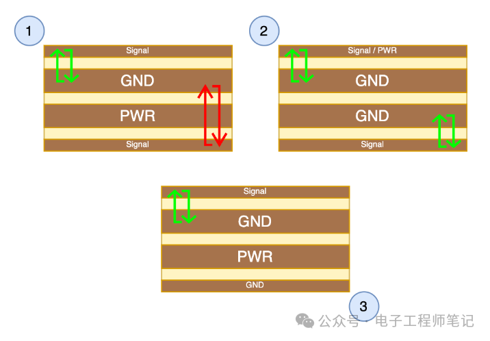
This diagram illustrates three possible arrangements of layers in a four-layer PCB design.
By using the bottom layer as the ground (GND) and power plane, and the top layer as the signal layer, with an additional ground (GND) layer placed directly below the signal layer, a very low-impedance PDN can be achieved. This approach is beneficial for designs with high current consumption or fast-switching components.
Ground Plane Design in Mixed-Signal Designs
In mixed-signal PCB designs, the ultimate goal of ground plane design is to isolate and separate mixed-signal areas as much as possible to prevent interference. If this is not achievable, designers should ensure that digital circuits do not induce currents in the analog portion of the PCB, as analog circuits are typically more susceptible to noise.In modern designs, it is generally not recommended to physically separate the GND plane into multiple smaller planes to avoid undefined return current paths between planes causing issues. Instead, complete isolation should only be performed when physical separation of GND signals is required for regulatory or physical reasons, such as in safety-critical applications, isolated power converters, or high-power applications.
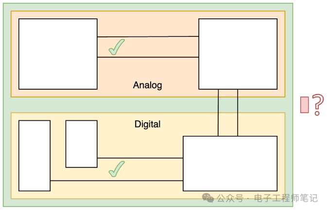
The return current paths directly above each area are clearly defined, but the exact behavior of the gaps between isolated reference planes is difficult to assess.
In mixed-signal A/D circuits, multiple ground layers may provide different references for different signal categories. However, in this case, designers typically want to connect the GND networks at a single point using a network connection. Therefore, the primary goal is not physical isolation but preventing digital noise from affecting the more susceptible analog subcircuits on the PCB.
Considerations for Designing Isolated Ground Planes
If physical isolation of AGND and DGND areas is desired or required, designers must route only digital signals above the appropriate digital reference plane. Similarly, analog traces must be located above the analog GND plane to prevent EMI issues and signal crosstalk between the two areas.If network connections are necessary, they should be placed in locations that do not allow any return currents from one type of signal to enter a different reference plane. When dealing with low-frequency analog and digital signals simultaneously, complete isolation is often easier to manage. In mixed designs with high-frequency analog subcircuits, network connections may be more appropriate.For isolated power converters, primary and secondary GND networks should be connected in different ways – for example, using very high-value safety capacitors that allow noise from the output side to return to the input side through the capacitors while maintaining the isolation barrier.
The Role of Via Stitching and Its Impact on Traces
Via stitching is a technique that connects copper planes on different layers of the PCB using vias. This method helps maintain short, low-impedance current loops and creates low electromagnetic noise areas, which is desirable in RF designs.However, it is crucial to consider the potential impact of vias on nearby traces and planes. Vias can introduce impedance discontinuities, reflections, and crosstalk, especially at high frequencies. Additionally, vias can create gaps in solid reference planes, disrupting the current loops of nearby traces. Therefore, careful layout and routing are necessary to mitigate these effects and ensure optimal PCB power distribution network performance.
The Bottom Line
Power planes help reduce noise and electromagnetic interference (EMI) and maintain signal integrity. However, due to the physical characteristics involved in electronic devices, power planes also present additional challenges. Designers must carefully consider and plan the current return paths and their effects on adjacent components and conductive layers, especially in mixed-signal designs.Several methods can help mitigate these issues. One of the most common methods is layer stack optimization, where designers can change the arrangement of layers in multilayer designs to move signal layers above reference planes. This ensures shorter, lower-impedance return paths to ground (GND). Well-placed decoupling capacitors can also achieve similar effects.In mixed-signal designs, one way to overcome signal degradation is to disperse low-frequency analog and digital components as much as possible. Separate ground planes are typically only recommended when physical isolation is required or necessary, such as for safety regulations. Instead, designers should adopt other methods, such as single network connections or safety capacitors. Via stitching also helps create low-noise areas in mixed-signal PCB designs.