“ In the previous article (Why is Circuit Grounding Design Important on PCBA?), we discussed three factors that lead to common impedance coupling interference: the non-zero impedance characteristics of the common return path; multiple systems sharing a common return path; and the low noise tolerance exhibited by circuits due to their unbalanced characteristics. This article mainly focuses on analyzing how to control common impedance interference on PCBA from the perspective of reducing the impedance of the common return path (common impedance)..”
01
—
Understanding Common Impedance
Most systems use AC signals, so it is necessary to consider not only the resistive characteristics of the return conductor but also its reactive characteristics. Therefore, reducing common impedance becomes a matter of reducing both resistance (R) and reactance (XL=ωL, ω=2πf). As shown in the following formula ( the AC resistance and reactance of conductors vary with frequency due to the skin effect, which must be considered in EMC grounding design—skin effect and proximity effect (a must-know in PCB design engineering)):
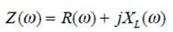
Where Z(ω), R(ω), and XL(ω) represent the frequency-dependent impedance, resistance, and reactance, respectively.
02
—
DC Resistance
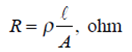
The definition of DC resistance is straightforward: the DC resistance R (Ω) of a conductor with a uniform cross-section is proportional to the material’s resistivity ρ (Ω×mm²/m) and the length L (m) in the direction of current flow, and inversely proportional to the cross-sectional area A (mm²), as shown in the following formula:
03
—
AC Resistance
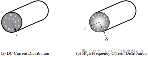
DC current is uniformly distributed across the cross-section of a conductor, while AC current tends to concentrate near the surface of the conductor. The higher the frequency, the greater the current density near the surface due to the skin effect. The definition of skin depth is: the depth at which the current density decays to e-1≈1/2.718 or 37% of its value at the surface. As the effective cross-section available for current flow decreases, the resistance increases. For circular conductors, the skin effect is illustrated as follows.
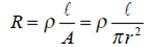
The DC resistance of a circular conductor can be expressed as:
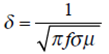
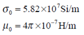
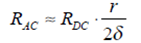
For conductors with a radius at least three times the skin depth, the skin depth δ is determined by the following formula (frequency is in Hz):

The effective cross-section for current flow is approximately:
AC resistance can be expressed as:
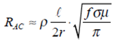
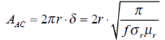
AC resistance can be approximately expressed as:
For a given cross-section, circular conductors have the minimum perimeter. Therefore, compared to flat conductors with equal area rectangular cross-sections, circular conductors have higher AC resistance (which is why grounding cables are often flat to reduce grounding resistance).
04
—
Reactance
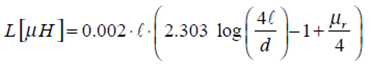
At high frequencies, reactance dominates, and this reactance is typically inductive. For conductors with a circular cross-section, length L, and diameter d (both in cm) and relative permeability µr, the internal inductance at low frequencies can be expressed as (assuming the current is uniformly distributed across the conductor’s cross-section):
As the frequency increases, the limit of inductance LHF approaches:
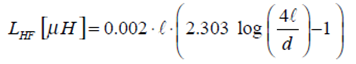
The above equation indicates: inductanceL increases linearly with cable length, while an increase in diameterd will reduce total inductance (which is a slowly varying function).
When using straight flat conductors instead of circular conductors, the internal inductance of the conductor is expressed as (assuming the widthw is more than 10 times the thicknesst):
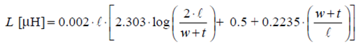
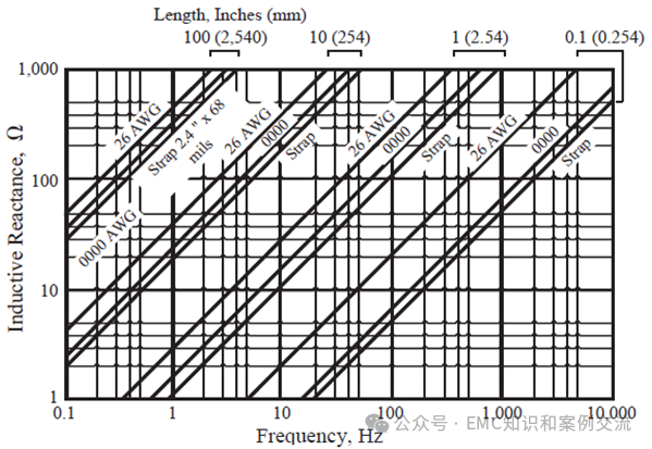
When comparing the internal inductance expressions of circular conductors and straight flat conductors, it is found that: in straight flat conductors, the aspect ratio (L:w) has a significant impact on inductance, resulting in flat conductors having lower impedance at high frequencies. The following diagram illustrates the internal inductance advantage of straight flat conductors over circular conductors.
05
—
Conclusion
From the above formulas and comparisons, the main measures to reduce common impedance are:
(1)Reduce conductor length;
(2)Increase cross-section;
(3)Use parallel conductor structures;
(4)Prefer flat conductors whenever possible.
Thank you for your feedback and suggestions.
———————————————
For more content, please follow our public account.