The PCB industry chain is structured as follows: Upstream Raw Materials — Midstream Substrates — Downstream PCB Applications
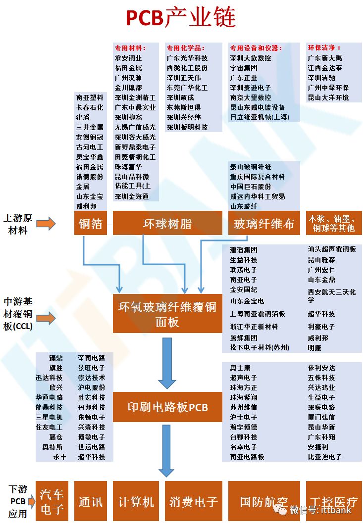
Upstream Raw Materials
Upstream raw materials include copper foil, resin, fiberglass cloth, wood pulp, ink, and copper balls, among which copper foil, resin, and fiberglass cloth are the three main raw materials.
Copper foil is the primary raw material for manufacturing copper-clad laminates, accounting for about 30% (thick boards) and 50% (thin boards) of the cost of copper-clad laminates. The price of copper foil is highly dependent on fluctuations in copper prices, significantly influenced by international copper prices. Copper foil is a cathodic electrolytic material that precipitates on the substrate layer of the circuit board, serving as a conductor in the PCB for electrical conduction and heat dissipation.
Fiberglass cloth is also one of the raw materials for copper-clad laminates, woven from fiberglass yarn, accounting for about 40% (thick boards) and 25% (thin boards) of the cost of copper-clad laminates. In PCB manufacturing, fiberglass cloth acts as a reinforcing material to increase strength and insulation. Among various fiberglass cloths, synthetic resin primarily serves as an adhesive to bond the fiberglass cloth together.
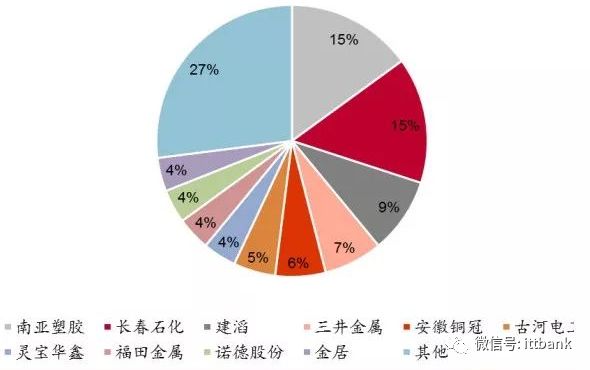
The production capacity share of the top ten electrolytic copper foil manufacturers globally
The copper foil production industry is highly concentrated, with leading companies having strong bargaining power. The copper foil used in PCB production is primarily produced through electrolysis, which involves a lengthy process with strict processing requirements, capital, and technical barriers. After several rounds of consolidation, the industry has become highly concentrated, with the top ten global copper foil manufacturers accounting for 73% of production, giving them strong bargaining power over the entire copper foil industry. Price increases in upstream raw materials like copper can be passed down. The price of copper foil affects the price of copper-clad laminates, which in turn leads to changes in PCB prices.
Midstream Substrates
Midstream substrates primarily refer to copper-clad laminates (CCL). Copper-clad laminates are made from raw materials such as copper foil, epoxy resin, and fiberglass yarn. The cost of raw materials accounts for a significant portion of PCB operating costs, approximately 60-70%.
Copper-clad laminates are the core substrate for PCB manufacturing. They are a sheet material made by soaking reinforcing materials in organic resin and covering one or both sides with copper foil, then thermally pressed. They serve three main functions in PCBs: conduction, insulation, and support. Copper-clad laminates are a type of special laminate specifically used for PCB manufacturing, accounting for 20% to 40% of the total PCB production cost, making them the highest proportion of material costs in all PCBs. Fiberglass cloth substrates are the most common type of copper-clad laminate, made with fiberglass cloth as the reinforcing material and epoxy resin as the adhesive.
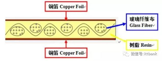
Diagram of copper-clad laminate structure
Downstream PCB Applications
Downstream refers to the various applications of PCBs, with decreasing industry concentration from upstream to downstream.
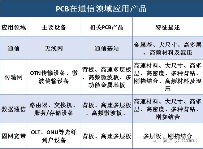
In the communication field, the application share increased from 22% in 2009 to 27% in 2017, showing a steady upward trend in PCB applications in communication, mainly used in devices such as mobile phones, optical modules, filters, communication backplanes, and communication base station antennas;
In the computer application field, the PCB output share gradually decreased from 32% in 2009 to 27% in 2016, mainly due to the gradual slowdown in growth in the computer industry;
In the consumer electronics field, the PCB application share has remained stable, maintaining at 14-15%, mainly used in products such as home appliances, drones, and VR devices;
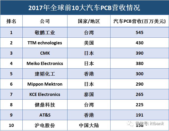
In the automotive electronics field, PCBs are mainly used in GPS navigation, car audio systems, car dashboards, and automotive sensors;
In the industrial control and medical fields, PCBs are mainly used in industrial computers, inverters, measuring instruments, and medical displays; in the aerospace field, PCBs are mainly used in aircraft, aerospace remote sensing systems, and aviation radar equipment.
Complete PCB Processing Process
Most engineers send PCB files or Gerber files to manufacturers and then wait for the boards to be returned. However, many hardware development positions may not have the opportunity to visit PCB production facilities to see the entire production process for many years.(This content is sourced from: Hardware’s Ten Thousand Whys)
Today, let’s take a look at the complete process.
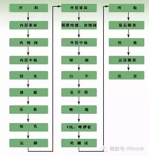
Step 1: Material Cutting
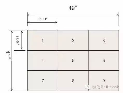
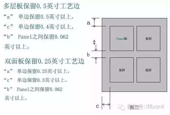
The raw materials for PCB factories are generally in sizes of 1020mm×1020mm and 1020mm×1220mm. If the size of the single board or panel is not suitable, a lot of raw material waste will be generated during the PCB production process. The PCB factory will add the cost of this waste to your board, making your PCB unit price higher. If the board size is well designed, and the single board or panel size is a fraction of the raw material, the utilization rate of the raw material will be maximized, allowing the PCB factory to cut the material efficiently, producing the most boards from the same raw material size, thus lowering the unit price.
We cut the purchased copper-clad laminates into the required sizes, which is called material cutting.
Cutting equipment: (cutting large boards into smaller boards)
The earliest copper-clad laminates were a dielectric layer with copper on both sides.
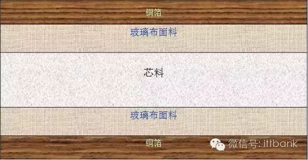
The above image is a cross-section of a copper-clad laminate.
Step 2: Layout
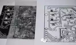
Step 3: Film
Import and modify the graphic files provided by the customer through software, and finally output the graphics onto film. This means converting the Gerber files you provided to the manufacturer into film.
Film refers to silver salt photosensitive film, also known as film. It is made from PC/PP/PET/PVC materials. Nowadays, it generally refers to photographic film, but it can also refer to negatives in printing. The film is usually black.
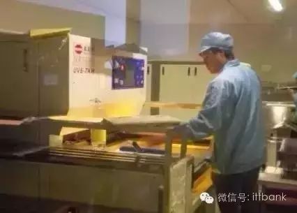
Step 4: Exposure
A layer of photosensitive liquid is coated on the surface of the copper-clad laminate, dried at 80 degrees, then the film is placed on the PCB, and exposed using a UV exposure machine, followed by removing the film.
The following image shows the exposure machine:
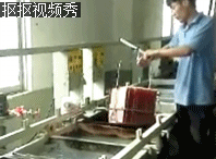
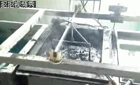
Step 5: Etching
The etching process can be broken down into the following steps:
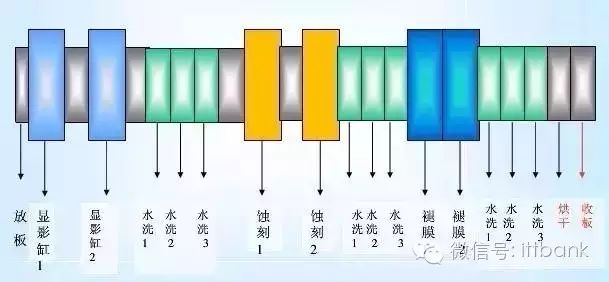
PCB etching machine
The board flows under the rollers
Why are the etching methods for inner and outer layers of PCBs different?
Inner layer: Development → Etching → Stripping
Outer layer: Development → Copper plating → Stripping → Etching → Stripping
Why is this done? Isn’t the outer layer etching process more complicated?
The inner layer generally has larger line widths and spacing, so a ring is sufficient; the outer layer generally has denser lines with limited space, so it is necessary to find ways to achieve the desired line layout within the limited space. Alkaline etching can achieve a 1-2 mil ring, but acid etching requires about 5 mils, so it is necessary to protect the required lines with tin. Wherever possible, alkaline etching should be avoided because it is more expensive than acid etching. The etching factor is a factory’s manufacturing capability and cannot be improved through processes. The etching capabilities of acid and alkaline etching differ.
Step 6: Drilling
The machine drills holes in the PCB according to the sizes and coordinates specified in the files.
For non-metallic holes, the PCB factory must use dry film or perform secondary drilling or plug with glue particles. Regardless of the method, it will increase the cost for the board factory. Therefore, if you do not specify, the factory will generally make metalized holes for you.
Step 7: Copper Plating
Copper plating involves depositing a layer of chemical copper on the non-conductive substrate (hole walls) and copper surfaces.
Step 8: Green Oil and Characters
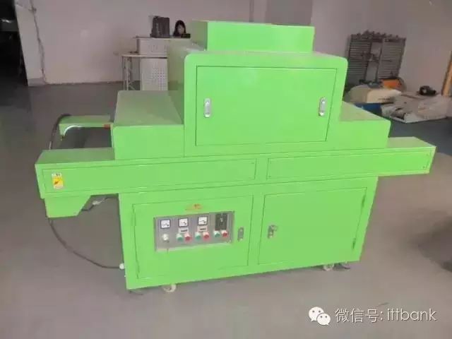
PCB low-temperature UV machine, purpose: UV coating curing
Character brushing:
Character screen printing 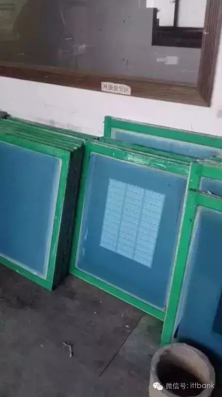
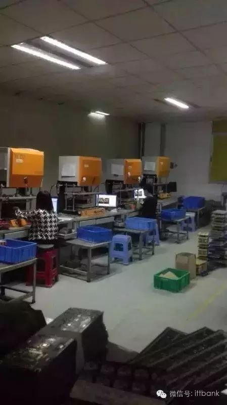
Final Step: Comprehensive Inspection
During sample processing, the factory generally does not use fixtures for testing, relying on manual testing; if in small batches, the factory needs to create test fixtures to test the impedance and connectivity of all traces.

PCBs are mainly divided into rigid boards (single-sided/double-sided/multilayer), flexible boards, HDI substrates, IC packaging substrates, and metal substrates.
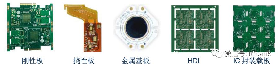
▲ Diagrams of various printed circuit boards
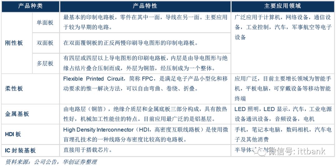
▲ PCB product characteristics and application fields
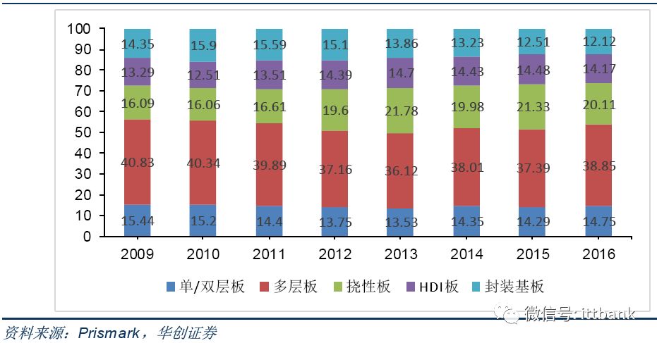
▲ Product structure and changes in the global PCB market (%)
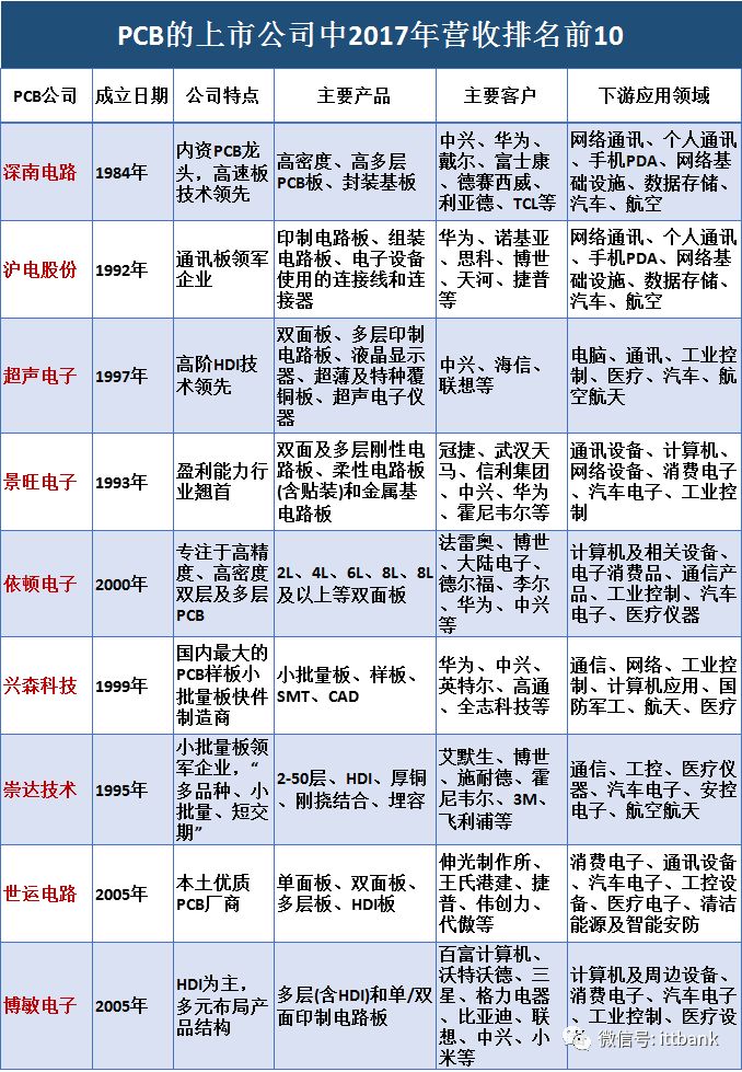
Shennan Circuit: Established in 1984, a leading domestic PCB company. It has three business segments: printed circuit boards, packaging substrates, and electronic assembly. The company has significant advantages in high-density, high-layer PCB products, capable of achieving up to 100 layers and a thickness-to-diameter ratio of 30:1. Revenue from the downstream communication sector accounted for over 60% in 2017.
Huada Technology: Established in 1992, a leading company in communication boards. Its products mainly include single-sided, double-sided, and multilayer boards, HDI, and circuit board assembly. The main products are 14-28 layer communication market boards, with the communication market boards being the primary source of revenue, accounting for 63% in 2017.
Ultrasonic Electronics: Established in 1997, a leader in advanced HDI technology. Its products include double-sided and multilayer printed circuit boards, LCDs, ultra-thin and special copper-clad laminates, and ultrasonic electronic instruments, serving as a long-term supplier for globally renowned companies such as Apple, Bosch, and Valeo. PCBs are the main source of revenue, accounting for 53% in 2017.
Jingwang Electronics: Established in 1993, known for its profitability in the industry. Based on rigid circuit boards, it has expanded into flexible circuit boards (including assembly) and metal substrates. It has developed production technologies for rigid-flex PCBs, high-density rigid-flex PCBs, and metal-based heat dissipation rigid-flex PCBs. Rigid circuit boards are the main source of revenue, accounting for 59% in 2017.
Yidun Electronics: Established in 2000, focusing on high-precision, high-density double-sided and multilayer PCBs. Its main products include 2L, 4L, 6L, 8L, and above. Major clients include Huawei, Flextronics, and Jabil. The 4L board is the main source of revenue, accounting for 47% in 2017.
Xingsen Technology: Established in 1999, the largest manufacturer of PCB samples and small batch boards in China. The company has become a core supplier of sample boards for Huawei and ZTE, and is a well-known brand in the domestic mid-to-high-end PCB sample and small batch board manufacturing field. Small batch and samples are the main sources of revenue, accounting for 77% in 2017.
Chongda Technology: Established in 1995, a leading enterprise in small batch boards. Its products cover 2-50 layers, HDI, thick copper, rigid-flex, and buried capacitor circuit boards. It positions itself with a business strategy of “variety, small batch, and short delivery time,” with a very short cash turnover period and outstanding operational capabilities. The customer structure is diversified, with over 70% of products exported to Europe, America, Japan, and Asia-Pacific regions. It has successfully transitioned from small batch boards to large batch boards, with large batch board revenue accounting for 57% in 2017.
Shiyun Circuit: Established in 2005, its main products include single-sided, double-sided, multilayer, and HDI boards, widely used in computers and peripheral devices, consumer electronics, automotive electronics, industrial control, and medical devices. Multilayer boards are the main source of revenue, accounting for 55% in 2017.
Bomin Electronics: Established in 2005, it has gradually formed a product structure centered on HDI boards, covering multilayer, single/double-sided, flexible circuit boards, rigid-flex boards, and other diversified products, with major clients including Baidu, Watford, and Samsung Electronics. HDI is the main source of revenue, accounting for over 50% in 2017.
———— / END / ————
Note: Personal sharing is welcome, please indicate the source when reprinting!
Submission email: [email protected]
ITTBANK customer service hotline: 25839333