In the process of developing and producing electronic products, one may encounter the scenario of needing to disassemble an existing PCB circuit board to analyze the circuit layout, component selection, and signal routing. Below, we will discuss an efficient process for disassembling a PCB circuit board, which we hope will be helpful to everyone.
1. Preparation Stage
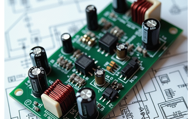
Record component information: Use a digital camera to take photos of the front and back of the PCB, and document all component models, parameters, and positions, especially the orientation of diodes, transistors, and the notch direction of ICs.
Remove components: Carefully remove all components using a hot air gun or solder sucker, ensuring that the solder residue in the PAD holes is cleaned out.
2. Cleaning and Drying
Clean the PCB: Use alcohol or a specialized cleaning agent to clean the surface of the PCB, removing residual flux, solder debris, and other impurities.
Drying process: Place the cleaned PCB in a ventilated area to air dry naturally, or use a hairdryer on low speed to dry it.
3. Scanning and Image Processing
Scan the PCB: Use a high-resolution scanner to scan the silkscreen side of the PCB into the computer, saving it as a high-quality image file (e.g., BMP format).
Image processing: Use image processing software (such as Photoshop) to adjust the contrast and brightness of the image, ensuring a strong contrast between the copper areas and non-copper areas. Then convert the image to black and white and check if the lines are clear.
4. Convert File Format
Convert to PCB design software format: Use professional PCB design software (such as Altium Designer, Protel, etc.) to convert the black and white BMP image file into an editable PCB file.
Align layers: In the PCB design software, check and align the PAD and VIA positions of the TOP and BOTTOM layers to ensure the accuracy of the conversion.
5. Draw the Circuit Diagram
Trace lines: In the PCB design software, trace the circuit lines on the TOP and BOTTOM layers based on the scanned image and the original component layout.
Place components: Based on the recorded component information, place the corresponding component symbols in the PCB design software, adjusting their positions and orientations to match the original layout.
6. Verification and Output
Electrical rule check: Run an electrical rule check (ERC) in the PCB design software to ensure that the circuit connections are correct.
Output files: Output the completed PCB file in the required format (e.g., Gerber files, PCB files, etc.) for subsequent PCB manufacturing or analysis.
This is an original article by Fan Yi Education, please indicate the source when reprinting!