1. What is a Reference Point (Mark Point)?
Mark point is also known as a reference point or optical positioning point, which is used as a positioning point by pick-and-place machines. Since PCBs provide a common measurable point for all steps in the assembly process during mass production, every device used in assembly can accurately locate the circuit pattern for precision. Through mark points, programmers can automatically set the machine after loading the program.
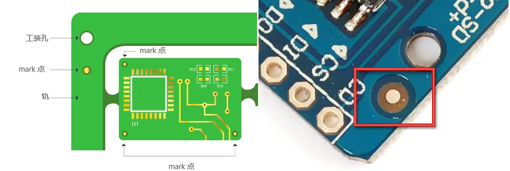 Mark Point
 Mark Point
2. The Role of Mark Points on PCB Boards
When we want to produce a board, we send the Gerber file to the manufacturer. If we need to assemble components with the PCB, we also need to provide a bill of materials (BOM file) and coordinate files (PNP file). These files will be used by automatic pick-and-place machines to obtain this information, and then a physical point or points on the PCB must be found.
Using mark points on the circuit board allows the machine to place components better, with higher accuracy, and does not rely on machine tolerances or human errors.
Mark Point
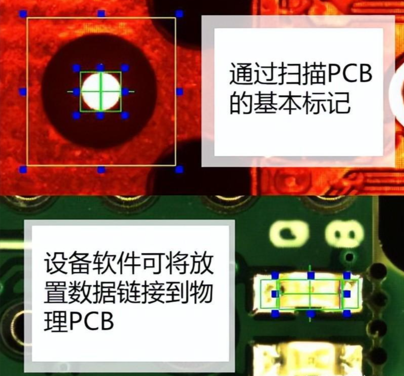
3. The Principle of Mark Point Recognition
Mark points on PCBs are reference standards used by automated machinery such as Surface Mount Technology (SMT) and Automated Optical Inspection (AOI). The mark consists of a single copper pad that is away from any other visible landmarks. Without a reference mark, the machine either places components incorrectly or refuses to operate entirely. However, by reading the positions of various reference marks placed on the PCB, automated devices can determine the exact position for placing or scanning components.
However, most machines technically do not read the content placed on the PCB; instead, they recognize the reflection of the mark point pads.
4. Different Types of Mark Points
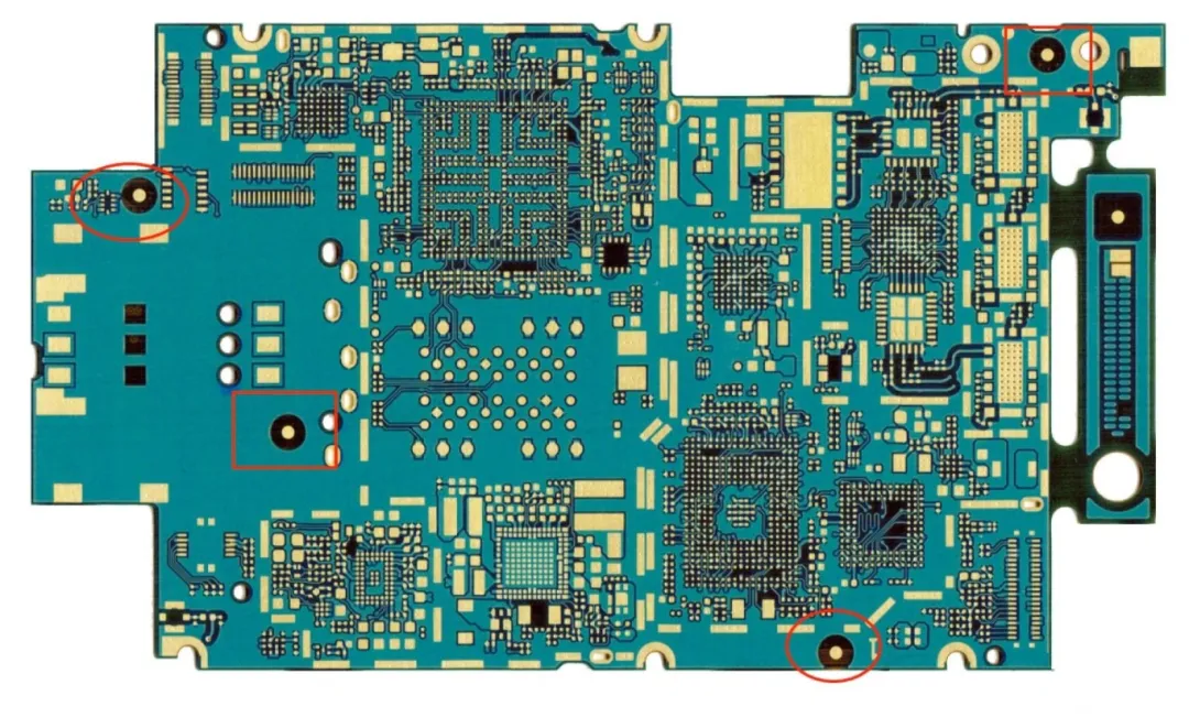
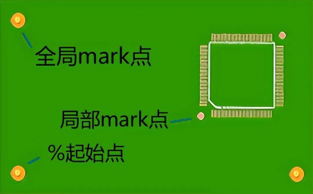
1. Global Mark Points
The role of global mark points is to locate all circuit features on a single board, distinguishing circuit patterns from PCB references, based on a three-network system where the reference point is located at the lower left corner (0.0), with the other two in the positive direction of the X and Y axes.
 Global Mark Point
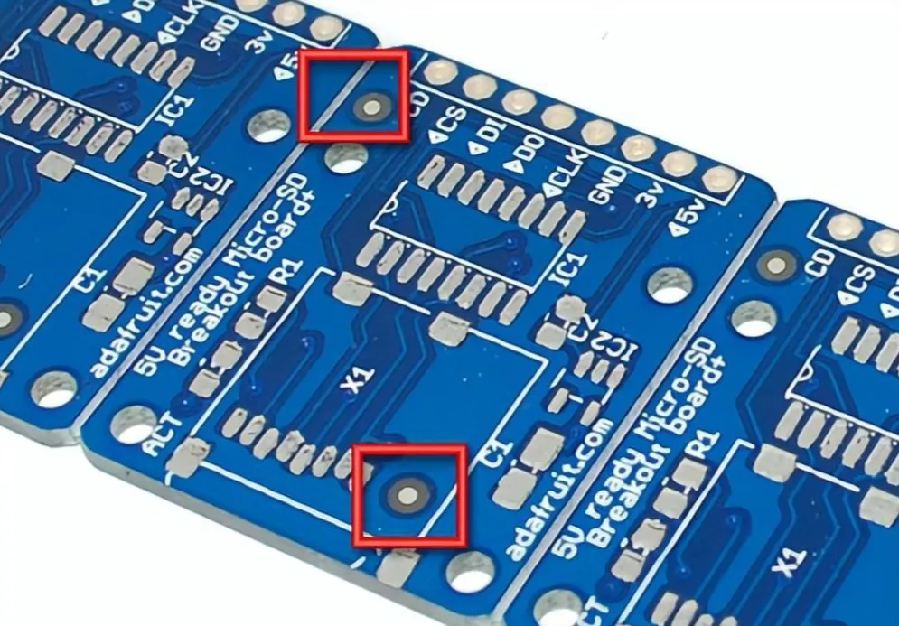
2. Local Mark Points
Local mark points are mainly used to locate components with many pins and small pin spacing (where the distance from the center is no more than 0.65mm), assisting in positioning.
Local Mark Point
3. Process Edge Mark Points
These are used on spliced boards to assist in locating all circuit functions.
 Process Edge Mark Point
5. General Principles and Steps for Mark Point Positioning
1. Mark Point Shape
After selecting the position of the reference mark, you can decide how they will be displayed. Although some manufacturing equipment is programmed to recognize various shapes, such as diamonds, squares, or hourglass shapes, not all machines can handle them. It is still recommended to use the more common circular mark points.
Why are circular mark points usually used?
● Circular objects are easier for machines to locate.
● For HAL completion, a convex shape on a circular reference will still be circular, while on a square reference, for example, it may no longer be square.
● Machines find the center of a circle more easily.
● Circular shapes have the smallest surface area.
● Uniformly etched circular shapes.
● Multiple reference points can be used instead of less efficient irregular reference points, which theoretically may contain rotational information but are difficult to process.
● This is a feature that differs most from traditional circuit boards, which are primarily rectangular.
● Circular mounting holes can also serve as inexpensive references.
Machine vision needs to accurately find the reference point and then estimate its exact center; circles are optimal.
 Mark Point Shape
2. Mark Point Size
Reference marks can come in various sizes, mainly depending on the assembly machine used.
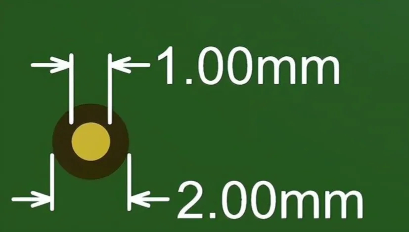
Sizes of 3.2mm solder mask opening diameter and 1.6mm bare copper diameter or 2mm solder mask opening diameter and 1mm bare copper diameter are generally suitable for all machines.
The size of reference marks on the same printed circuit board should not exceed 25 µm, and the minimum size of the gap area is recommended to be twice the radius of the center mark.
A blank area should surround the reference point, with no other circuit elements or marks. The minimum size of the blank area should be twice the radius of the reference point.
PCB reference sizes are typically between 1 to 3 millimeters, mainly depending on the assembly machines used by manufacturers. Some manufacturers recommend adding three reference points at the corners of the circuit board, as this provides two angular alignment measurements and allows the pick-and-place machine to infer the correct orientation. Some manufacturers specify exact sizes, which also depend on the assembly equipment used.
In general, the diameter of the solder mask opening should be twice the diameter of the bare copper reference, and additionally, the PCB reference sizes on the same board (global and local) should be consistent, with variations not exceeding ~25 microns.
If assembling a two-layer board, the reference points on the top layer and bottom layer should be directly above each other. The reference sizes for the top and bottom PCBs should be the same, including solder mask openings.
 Common PCB Mark Point Sizes and Solder Mask Opening Recommendations
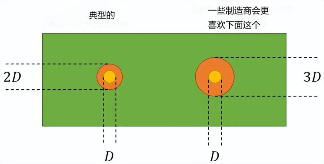
Local references are often as small as 1 millimeter, with a solder mask opening of 2 millimeters. The D-3D rule shown in the image above is preferred by some manufacturers for its larger solder mask opening.
Local PCB reference sizes typically do not exceed 1 millimeter to allow for routing and to leave space for other components. For small components like 0201 resistors or chip-sized BGAs, the assembly machine will be precise enough, so local references are not needed, and the machine will accurately know where to place your components.
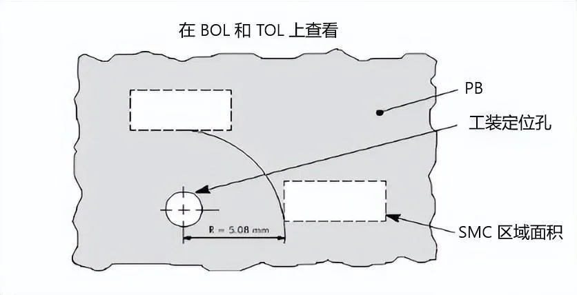
3. Mark Point Edge Distance
Avoid placing reference points close to the edge of the PCB, as mounting machines typically use fixtures to lock the PCB in place during assembly. If the fixture covers the reference point, it can cause serious issues. Reference marks can be placed at least 3 millimeters from the edge (5 millimeters is recommended to eliminate these risks).
Mark Point Edge Distance
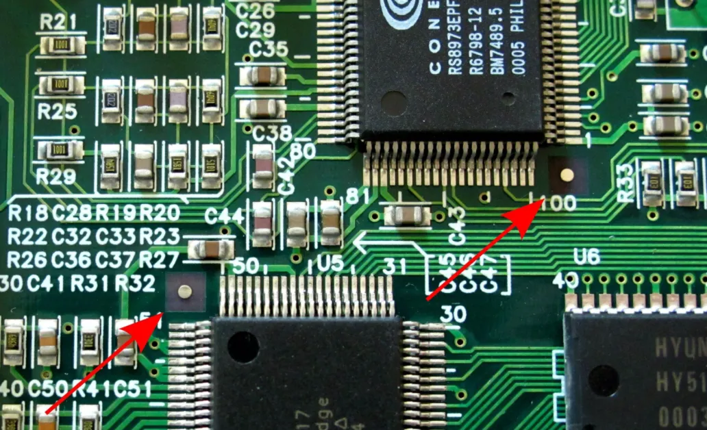
4. Mark Point Composition
Mark point composition consists of three parts:
● A solid copper ring on the top or bottom copper layer
● A circle in the solder mask layer that is the target we need to align with
● Side option text labels

Mark Point Composition
5. Mark Point Position Layout
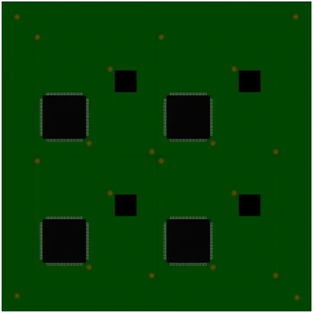
Mark points need to be located at the four corners or diagonally on the PCBA, forming multi-point surface positioning, with accurate positioning and as far apart as possible.
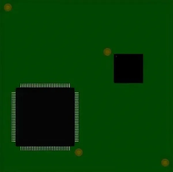
1) PCB Mark Points
The layout position of mark points is determined by the PCB transfer method of the pick-and-place machine. When using a rail to transport the PCB, marks cannot be placed near the clamping surface or positioning holes; specific dimensions vary by machine. General requirements are shown in the image below.
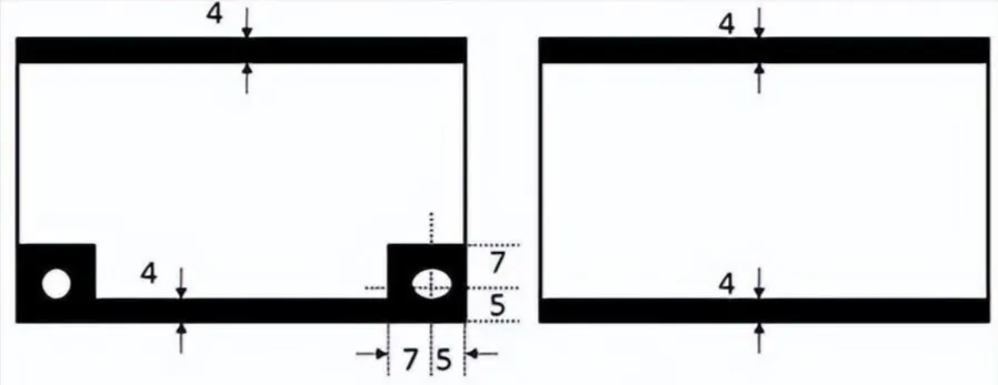 Area Mark Cannot Be Positioned
● During positioning, mark points cannot be located.
● During edge alignment, mark points cannot be positioned within 4mm of the edge. PCB mark point positions should be placed along the diagonal, and the distance between them should be as large as possible.
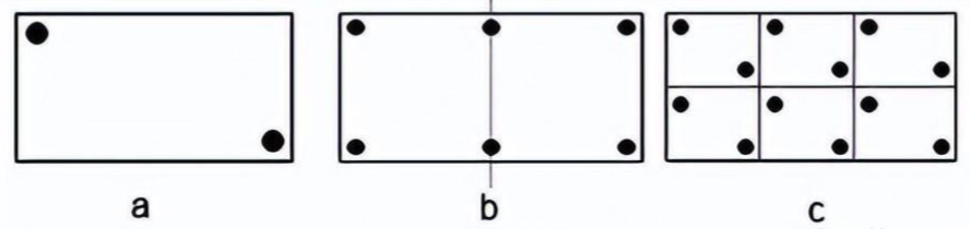
● For PCBs shorter than 200mm, at least 2 marks should be placed, as shown in the image. For PCBs longer than 200mm, 4 mark points need to be placed on the PCB along the centerline or near the centerline of the long edge.
PCB mark point marks should be placed along the diagonal of each small board, as shown in the image below.
 PCB Mark Point Position Layout
2) Local Mark Points
Local mark point positions should meet the following requirements: For QFP components with more than 100 pins, 2 mark points should be placed along the diagonal, as shown in image a. For QFP components with more than 160 pins, 4 marks should be placed at the four corners, as shown in image b.
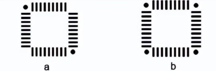 Local Mark Point
 Mark Point
6. Mark Point Cut Gap
The appropriate gap around the mark point is crucial. An open area (no copper, solder mask, silkscreen, etc.) should be placed around the pad. With this space, the camera can pick up the mark without visual interference.
The diameter of the open space should be at least twice the size of the pad. Therefore, for a 2mm pad, you need to leave at least a 4mm gap area around it. The shape of the gap area is not very important; circular and square areas are two popular designs.
 Mark Point Cut Gap
7. Mark Point Material
Mark point pads need to be made of the same metal as the rest of the circuit board. (Remember, the pad is used to reflect light.) Therefore, do not cover the pad with solder mask, silkscreen, or any other material.
8. Number of Mark Points
The number of three reference points is the best number to eliminate unexpected misalignment of the template relative to the PCB.
1) One Mark Point
With only one reference mark available, the scanning software cannot determine the correct rotation of the PCB. A machine cannot effectively operate with only one reference mark on the PCB.
2) Two Mark Points
With two reference marks available, the machine can operate normally. However, there are two risks at play here.
● A dual mark setup provides good but often not very accurate position tracking. If fine-pitch components are used, it may not be that accurate.
● Conversely, opposing reference points may lead to operator errors. If the PCB is inserted upside down, the machine may still see the reference points and continue its operation. The best-case scenario for this mistake is wasted time, while the worst-case scenario could lead to catastrophic component stacking or permanent damage to the PCB and equipment.
3) Three Mark Points
Three is the optimal number of reference marks for correctly operating a PCB, as the third reference mark can add an extra point for triangulation, improving overall accuracy. It also eliminates any possibility of incorrectly rotated boards being processed by the camera.
4) Four Mark Points
While it seems that adding four points could further improve accuracy, there is rarely much to gain from this. The main downside here is that the fourth reference mark reintroduces the risk of processing inverted panels. Caution is advised when going this route.
 Mark Point
9. Mark Point Copper Finish
Mark point pads need to be smooth to reflect a uniform image, and the copper mark is plated with any metal finish of your choice. Processes like electroplating and immersion are reliable in terms of uniformity, while hot air soldering tends to have more variation.
 Mark Point Copper Finish
If there are any variations in the thickness of the finish, it cannot reflect correctly. While it is not insurmountable, it does force production operators to spend extra time recovering the marks. Depending on the severity of the issue, it may require editing the software program for compensation or completely re-soldering the reference points. In short, fixing this can take a significant amount of time.
10. Mark Point Contrast
Optimal performance is achieved when there is a high contrast between the mark point and the substrate material of the printed board. For all mark points, the internal background must be the same.
6. How to Create Mark Points?
Device hole interface devices and connectors are mostly through-hole components. The diameter of the through hole for the plug is 8 to 20 mil larger than the pin diameter, which ensures good solderability. It is important to note that there is a margin of error in the hole diameter when the circuit board is manufactured. The approximate error is ±0.05mm. Every 0.05mm is one drill. For diameters over 3.20mm, every 0.1mm is one drill. Therefore, when designing the device hole diameter, the units should be converted to millimeters, and the hole diameter should be designed as an integer multiple of 0.05. Manufacturers set the size of the drilling tools based on the drilling data provided by users. Drill sizes are usually 0.1-0.15mm larger than the molded hole requested by the user. The smaller, the better.
 Mark Point Creation
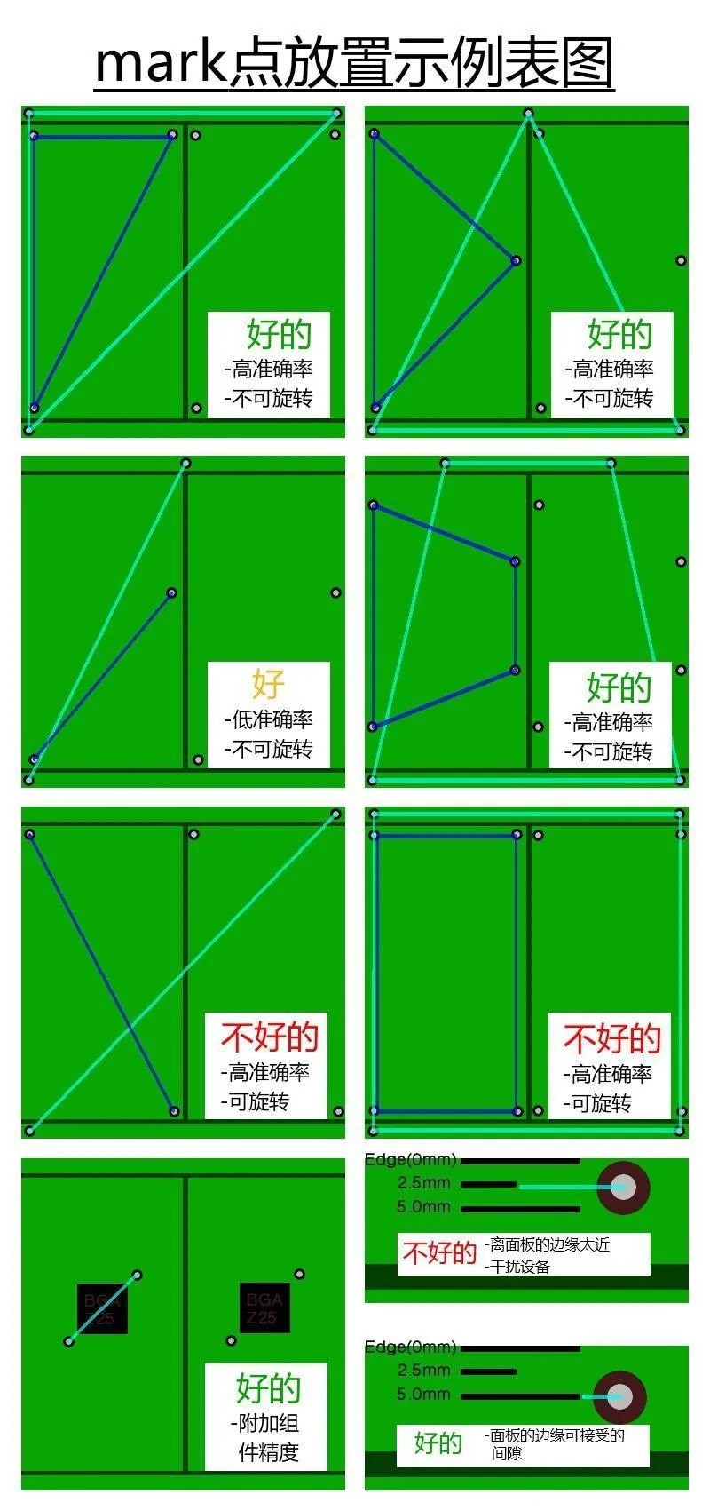
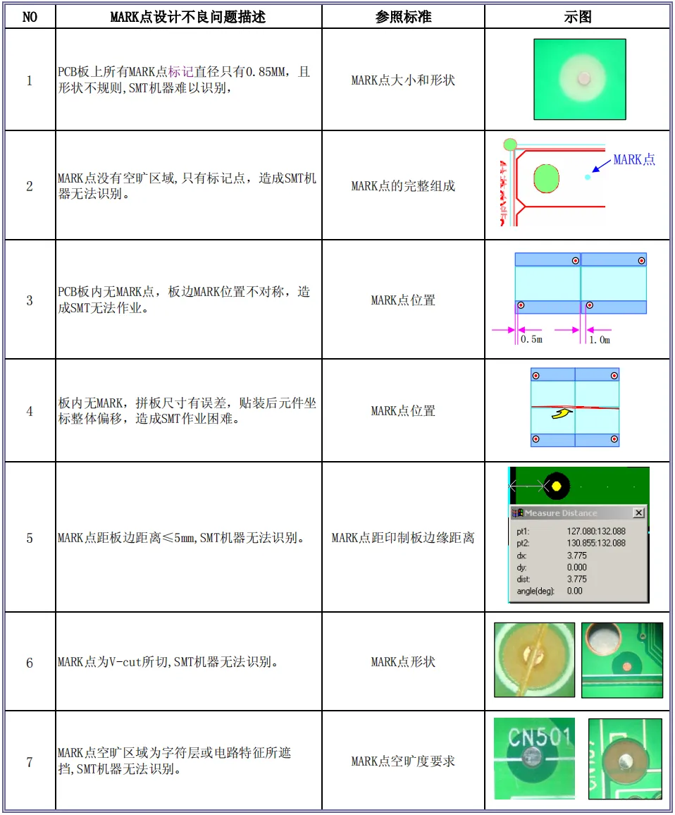
7. Examples of Poor Mark Point Design
 END
END
Disclaimer:This article is reproduced from the internet, and the copyright belongs to the original author. If there are any copyright issues, please contact us in a timely manner. Thank you!