The Seven Deadly Sins, seven sins in Catholicism, abbreviated as the Seven Deadly Sins. The term ‘sin’ refers to the source or root of something.
In Catholic doctrine, it is stated that “according to John Chrysostom and Pope Gregory I, we can discern the major evils that believers often encounter.” Here, ‘major’ means that these evils can lead to the occurrence of other sins, which are ranked in increasing severity as pride, envy, anger, sloth, greed, lust, and gluttony.
The First Sin of I2C
Some engineers, when discussing I2C, may exhibit a dismissive attitude, saying, “Come on, it’s just two wires, one for clock and one for data!” Every time I encounter such individuals, I feel like saying, “Dude, you really haven’t stepped in enough pits yet!”
Below, I will list the I2C issues I have encountered in chronological order based on my work experience. I want to emphasize that the problems I list are not derived from books or fabricated; each problem comes from different companies and projects, and I have personally experienced and resolved them. I hope they help young engineers!
In 2005, on a light network system at Company L (think back to the glory days of Company L), there was a peculiar issue with a line card called LKAXXX. At this point, some people might laugh at the mention of MPC860; you can tell they are older folks. Ah, time waits for no one ^_^. When I graduated from school, the MPC860 was just about to be born.
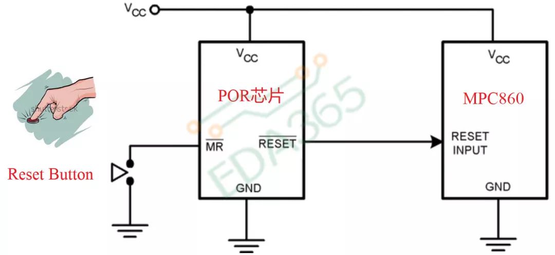
 Let me describe the problem:
1. Often when someone presses the Reset button, the system fails to boot; the UART console prints part of the information and then hangs;
2. Pressing the reset again results in the same symptoms; no matter how many times the reset button is pressed, the system freezes, with the UART printing a bit of information and hanging;
3. After multiple ineffective reset attempts, powering off and restarting works;
4. In most cases, pressing the reset button on the same board works, but in a few cases, it fails.
At this point, many would say, “Isn’t this simple? Just use a debugger to set breakpoints and trace!” That’s right, our firmware engineers are quite skilled and quickly tell us the problem lies with I2C. We measured the I2C signal with an oscilloscope during the hang and found that the SDA data line was continuously low; no matter how we reset it, it remained low. Only after power cycling did the SDA go high. Thus, the initial cause was identified: the I2C-SDA was being forcibly pulled low, preventing the system from booting, while power cycling released the SDA, allowing the system to function normally.
We know that I2C is open-drain, so it must be pulled low by some chip. It’s easy to think it shouldn’t be the CPU, as the CPU has already been reset. Thus, the suspects shift to the device connected to the CPU. At first glance at the schematic below, I thought, “What’s this? Is it a connect-the-dots game? Can it get any simpler?”
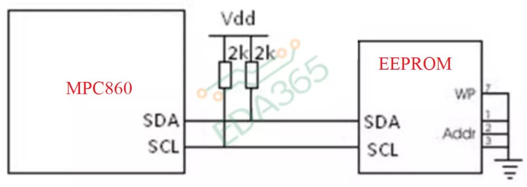
So what exactly caused the SDA to be pulled low by the EEPROM?
Let’s take a look at another diagram:
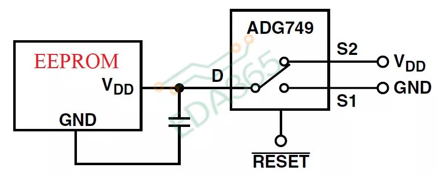
Here, we see that the treatment of the EEPROM is quite special. In most schematics, I’ve never seen it done this way: the EEPROM’s power supply is connected to a switch:
1. When reset is low, the EEPROM’s VDD is connected to low, powering it off;
2. When reset is high, the EEPROM’s VDD is reconnected to the external VDD, restoring power.
At this point, smart partners have figured it out: If every time we press the reset button to reset the CPU, the reset signal generated by the button (High-Low-High) disconnects the EEPROM’s power for a moment, wouldn’t the EEPROM stop pulling SDA low? Bingo, that’s right.
But then someone might say, “Doesn’t that increase costs? Also, I haven’t seen anyone do this before.” Haha, right. Only the Japanese would use such a rigid design method. We Chinese will always find a better solution. Let’s move on.
Take a look at the diagram below. Does it look familiar?
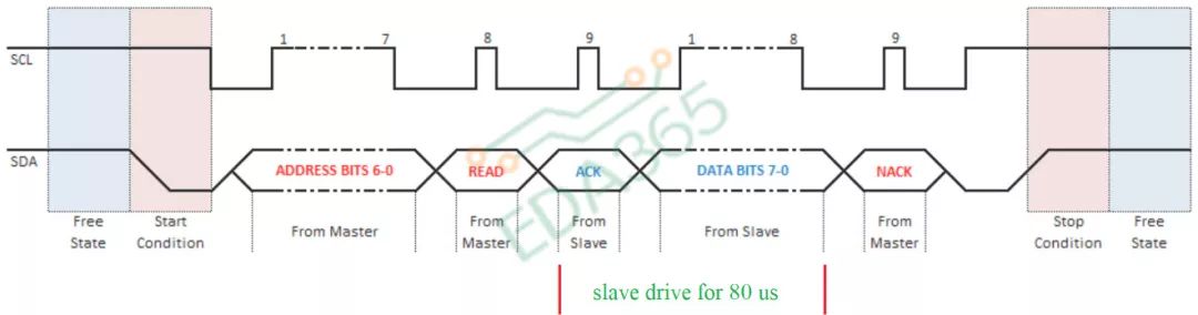
This is an I2C read operation, in the following sequence:
1. The Master issues a start;
2. The Master sends the address and read command;
3. The Slave gives an ACK and then sends data bits 7-0, a total of 8 bits driven by the slave on the I2C SDA (remember that SCL is always driven by the master, although there are special cases that we will detail in the later sins), and the time for the 8 bits (assuming a rate of 100K, with a period of 10us) is 80us.
Stop, stop, stop! Here comes the funny part: what happens if someone presses the reset button during these 80us?
 Let’s take an example:
Imagine four people playing Mahjong. After my opponent plays a tile, it’s my turn to play, but then I get a phone call and go to answer it. When I return to the table, I forget that it’s my turn, thinking the previous round is over, and I just push all the tiles down to shuffle. My next opponent is not happy because they were waiting for me to play to win. My actions annoy them, and no apology will suffice; they’re done! So, this round of Mahjong cannot continue.
Analogous to the I2C situation, imagine:
1. At 80us, the EEPROM Slave is happily outputting read data to the CPU;
2. At this moment, the CPU receives a reset instruction, a forced reset, similar to answering a phone call;
3. After the CPU resets, it completely forgets that the EEPROM was driving data, and it’s possible the EEPROM has already transmitted the 8bit data and is waiting for the CPU’s NAK (as shown in the diagram). Who could tolerate that?
4. In this situation, the CPU seems powerless; after all, we pressed the reset button. Another scenario is that the CPU might be unkind, such as executing a high-priority interrupt and then forgetting that the EEPROM was waiting for it to continue its previous operation.
Some might ask, “Wasn’t it reset?” Please carefully observe the schematic above; the EEPROM does not have a reset pin. This means that when we press the reset button, the CPU resets, but the EEPROM does not. Its state machine is still waiting to output data to the CPU or waiting for the CPU’s NAK instruction to end the current operation, which is analogous to the Mahjong example above.
So, what caused the SDA to be pulled low? It’s simple; the ACK in the diagram is a low level, or there are high and low bits in the data bits 7-0 driven by the Slave.
Besides adding a power switch to the EEPROM, do we have any other methods to solve this issue?
Let’s continue looking at the diagram:
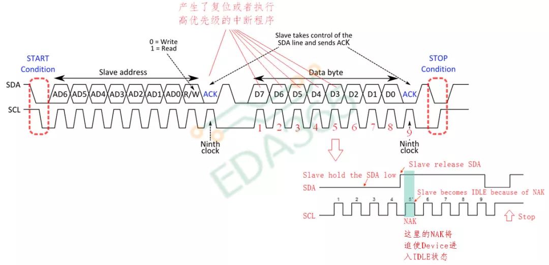
Let’s think about the Mahjong situation again. If I give each of my friends 100 yuan after finishing my Mahjong game, they would definitely be happy to continue playing with me. A simple solution resolves the problem. As shown in the diagram, we had the software engineers make a modification in the code:
1. When SDA is detected to be pulled low;
2. The software continuously sends 9 clock pulses;
3. During the 9 clock pulses, SDA will go high and low;
4. When the device has sent all data, SDA is released;
5. At this point, when the state machine reaches the NAK phase, SDA is released and goes high, generating a NAK;
6. Note that the 9 clock pulses may not be fully utilized; the EEPROM may release SDA upon reaching the NAK phase, but the CPU will continue to send all 9 clock pulses;
7. Finally, the CPU sends a stop condition to terminate the entire read operation;
The 9 clock pulses make the hanging device’s state machine move to the next state after each clock pulse while SDA is released (not pulled down), which will cause a NACK when the state machine moves to the ACK phase. The NACK will force the device to go to idle mode (which is consistent with the steps I mentioned above).
1. The Master tries to assert a logic 1 on the SDA line;
2. The Master still sees a logic 0 and then generates a clock pulse on SCL;
3. When the device reaches the NAK phase, the master will generate SDA high, which is a NAK, but the master does not know until it sends all 9 clocks;
4. The Master generates a stop condition.
The above discusses the situation where an I2C read operation is interrupted, resulting in a hang. Now let’s talk about the situation where an I2C write operation is interrupted, which is a “simple and crude” solution. Everyone should think about why.
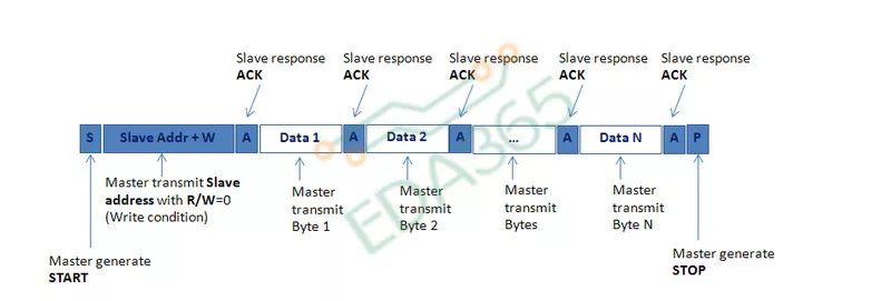
Here, we still send 9 clock pulses. During these 9 clock pulses, the device might send an ACK. After the CPU sees the ACK, it sends a stop to end the operation:

1. The Master tries to assert a logic 1 on the SDA line;
2. The Master still sees a logic 0 and then generates 9 clock pulses on SCL;
3. Generates a stop condition.
It is important to note that when a write operation is interrupted, the 9 clock pulses must wait until the last clock is completed before the device is released. In contrast, during a read operation, it may happen that the device is released after the first clock, but the CPU does not know this, and the stop occurs at the ninth clock.
The article concludes with a question for everyone: Why is it specifically 9 clock pulses? Feel free to leave your thoughts in the comments. If you understand this, you will have grasped the essence of this article.
