Image and text reproduced from:AI Electronics Circuit Home
A Printed Circuit Board (PCB) is a board-like component that forms circuit connections and component layouts on a common substrate according to specific design requirements through printing processes. As one of the core components of modern electronic devices, PCBs are known as the “mother of electronic products” and play a crucial role in electronic systems.
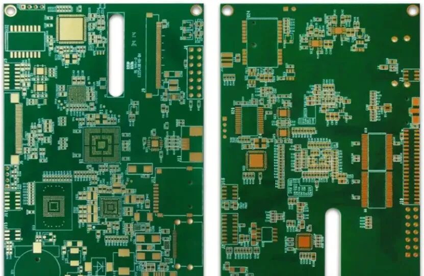
Its main functions include:
Mechanical Support: Provides a stable installation platform for various electronic components in the circuit, ensuring structural stability during use;
Electrical Interconnection: Achieves predetermined electrical connections between electronic components through precise circuit design and wiring, acting as a relay for signals and power;
Identification and Recognition: Clearly identifies the position and function of each component through labeled symbols and circuit diagrams, facilitating subsequent insertion, testing, and debugging work.
PCBs are widely used in various high-tech fields, including but not limited to semiconductor packaging, consumer electronics, automotive industry and automation control, medical devices, military and aerospace defense, making them one of the important foundations driving the development of modern electronic technology.
Classification of PCBs
Printed Circuit Boards (PCBs) can be classified in various ways based on different manufacturing materials, structural characteristics, and circuit design complexity. Below are several main classification methods and their characteristics:
1. Classification by substrate material
The substrate of a PCB, also known as Copper Clad Laminate (CCL), is the most basic material for making circuit boards, consisting of a laminated board with one or two sides covered with metal copper foil. Copper clad laminates are divided into rigid and flexible types. The substrate of copper clad laminate is a non-conductive insulating material. Copper clad laminate is formed by bonding copper foil/adhesive resin/paper or fiber cloth under heat and pressure.
Organic Material Boards
Composed mainly of organic polymer materials, such as polyimide (PI), polytetrafluoroethylene (PTFE), epoxy resin, etc. They have good electrical performance and processing adaptability, widely used in high-frequency, high-speed, and high-density interconnect (HDI) high-end fields.
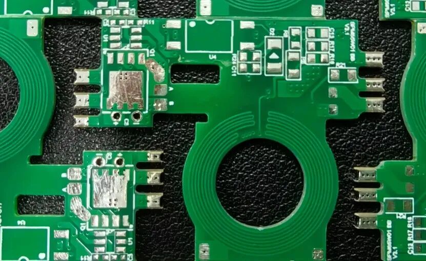
Inorganic Material Boards
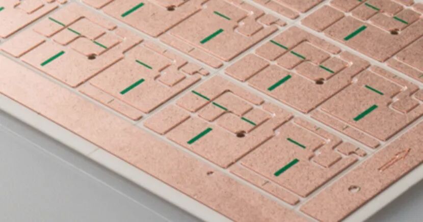
Primarily refers to ceramic substrates, which have extremely high thermal conductivity and insulation properties, suitable for high power, high temperature, and high reliability requirements scenarios, such as LED lighting, power modules, aerospace, etc.
2 Classification by substrate flexibility
Rigid Substrate (Rigid PCB)
The substrate is hard and not easily bent, providing structural stability, suitable for most conventional electronic devices. Common materials include glass epoxy resin (FR-4) and paper phenolic resin (FR-1).
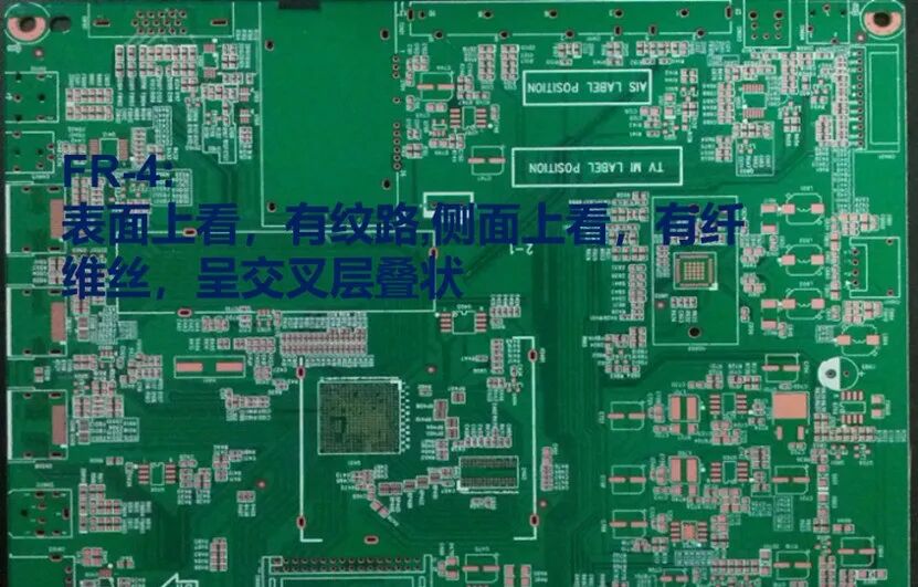
FR-4 (Glass Epoxy Substrate)
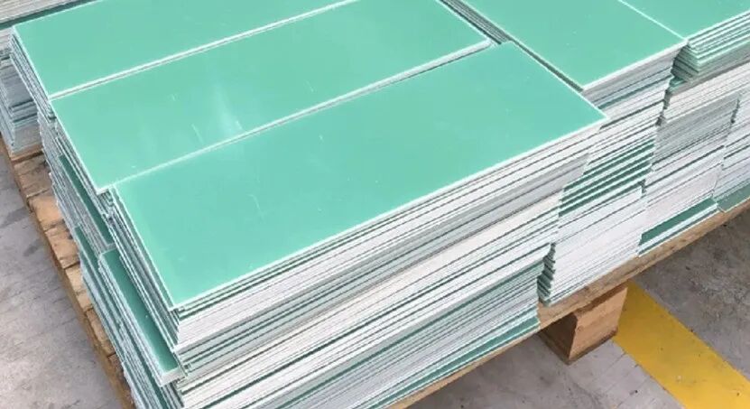
Made from glass fiber cloth impregnated with epoxy resin, it has good mechanical strength and insulation properties, is moderately priced, and is widely used in consumer electronics, industrial control equipment, etc. The downside is that it can produce burrs during processing, requiring careful process control.
FR-1 (Paper Phenolic Substrate)
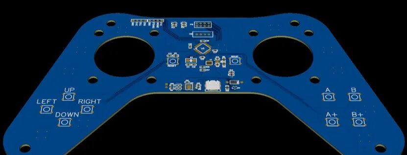
Paper phenolic substrates are made from paper scraps and phenolic resin, appearing flat like paper. This includes: FR-1, FR-2, FR-3, XBC, HB (FR-2 has higher electrical performance requirements and is more expensive than FR-1, but other properties are not significantly different. “FR” indicates that the resin contains flame-retardant substances, giving the substrate flame retardant (Flame retardant) or flame resistance (Flame resistance) properties).
Advantages: Low raw material cost, and due to its softer texture, it can be punched, resulting in lower processing costs during the circuit board manufacturing process.
Disadvantages: Relatively poor hardness, easily absorbs moisture in humid environments, and experiences significant thermal expansion and contraction changes (e.g., easily deformed during wave soldering), and its electrical performance is lower than that of fiber boards.
Among them, FR1 uses paper core material impregnated with phenolic resin, is inexpensive, and is suitable for low-cost electronic products with single-sided board structures, such as white goods, simple remote controls, etc. However, its durability is poor, prone to warping, and not suitable for multilayer board designs.
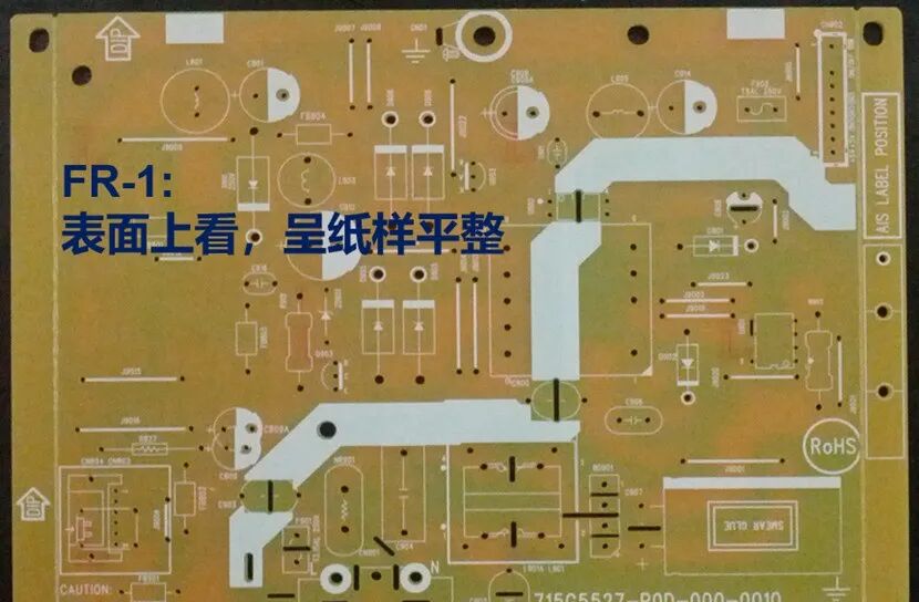
CEM Paper-based Epoxy Resin – Composite Fiber Board:
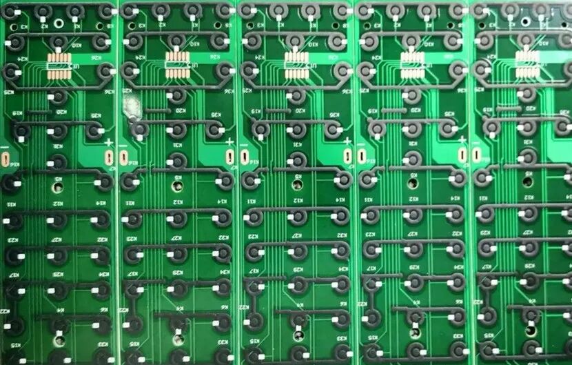
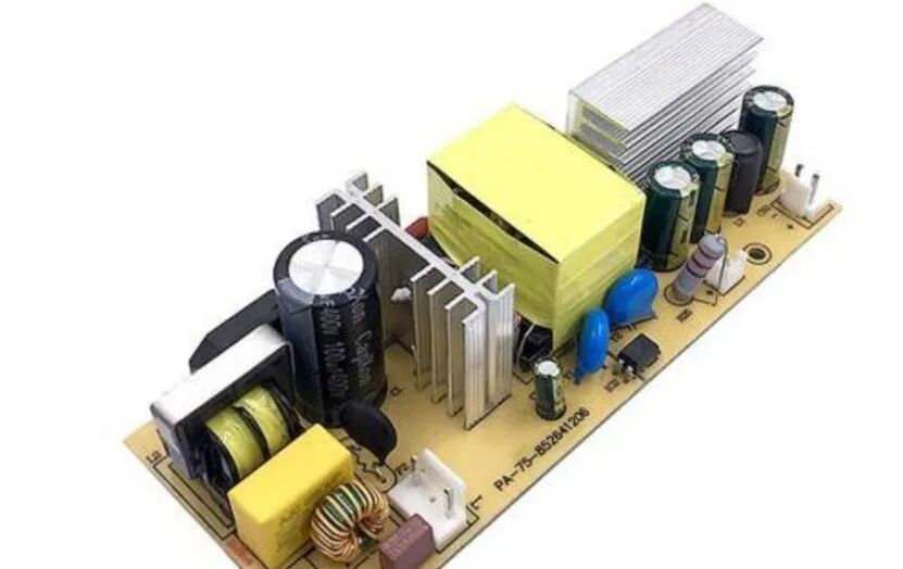
a Composition Characteristics: The substrate is made from a mixture of paper scraps and epoxy resin, with a glass fiber surface, pressed together, appearing textured.
b Includes: CEM-1 (Paper Core), CEM-3 (Glass Fiber Core).
CEM-1 consists of: Copper foil + Paper (Core) + Epoxy Resin (Core) + Glass Fiber Cloth (Surface),
CEM-3 consists of: Copper foil + Glass Fiber Non-woven Fabric (Core) + Epoxy Resin (Core) + Glass Fiber Cloth (Surface),
CEM-3 has more fiber layers than CEM-1, thus its flame resistance, insulation, hardness, etc., are higher than those of CEM-1, and it can replace FR-4 for some PCB double-sided boards and PCB multilayer circuit boards.
c Advantages: Composite fiber boards are cheaper than glass fiber boards, solving the hardness issue of paper boards and the difficulty of punching fiber boards.
d Disadvantages: Although the electrical performance is close to that of glass fiber boards, it cannot completely replace FR-4 materials; only some less demanding circuit boards can use this material as a substitute for FR-4.
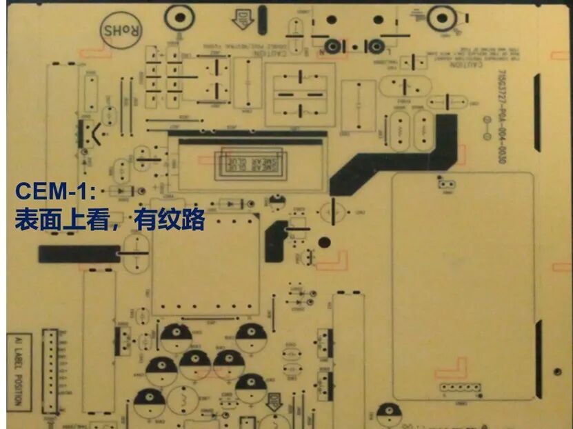
Flexible Substrate (Flexible PCB, abbreviated as FPC)
Made from flexible materials (such as polyimide PI, polyethylene terephthalate PET), it has good flexibility, lightweight characteristics, and adaptability to three-dimensional space, commonly used in devices with limited space or requiring flexible deformation, such as foldable phones, camera modules, flexible displays, wearable devices, and flexible solar cells.
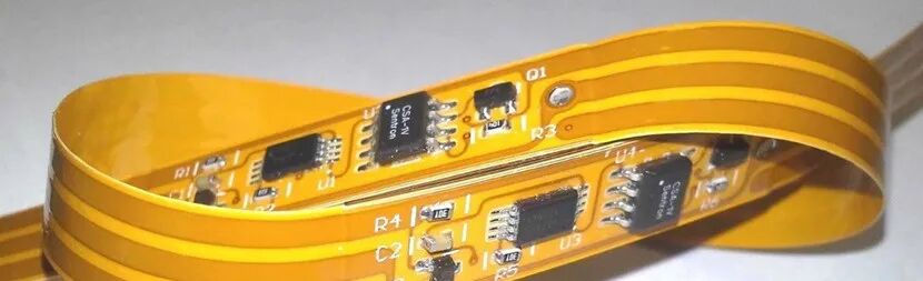
Rigid-Flex Substrate (Rigid-Flex PCB)
Combines the advantages of rigid and flexible boards, with some areas being rigid structures and others being flexible, suitable for high-density interconnect devices with complex structures, such as high-end communication devices, medical equipment, military electronics, etc.
3 Classification by number of copper foil layers
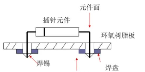
Single-sided Board (Single-sided PCB)
Only one side has copper foil circuits, suitable for simple circuit designs. Surface-mounted components and wires are on the same side, while through-hole components are on the other side. Due to limited routing paths, they cannot cross, and are usually used in early or structurally simple electronic products.
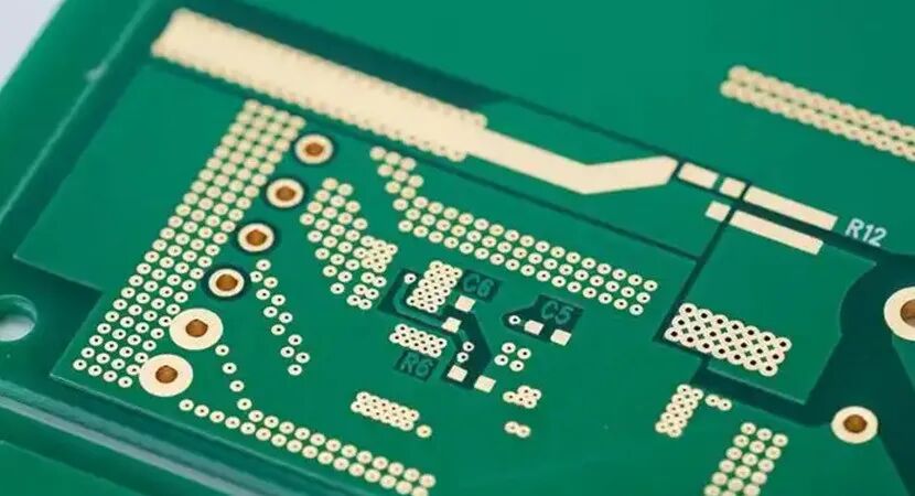
Double-sided Board (Double-sided PCB)
Both sides have copper foil circuits, and inter-layer connections can be achieved through vias, enhancing wiring flexibility and space utilization, suitable for medium complexity circuit designs.
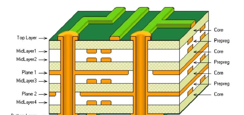
Multilayer Board (Multi-Layer PCB)
Composed of multiple single-sided or double-sided boards laminated together with insulating media, the number of layers can reach 4 layers, 6 layers, or even dozens of layers. Suitable for high-density, high-complexity circuit designs, such as high-performance computing devices, communication base stations, servers, etc.
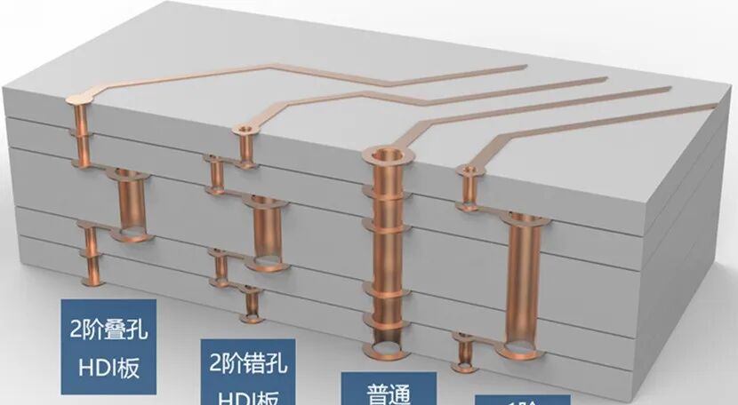
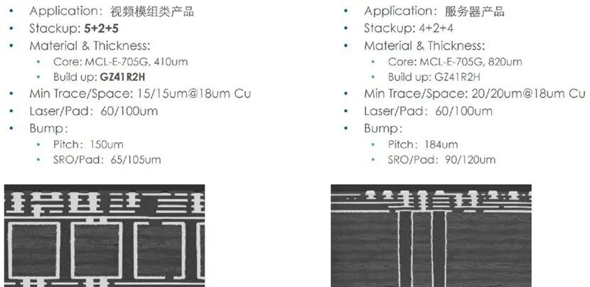
HDI Board (High-Density Interconnect)
Utilizes micro-blind holes, ultra-fine lines, and high-density interconnect technology, suitable for chip packaging, smartphones, AI servers, and other highly integrated electronic products. Compared to traditional multilayer boards, HDI boards can maintain lower manufacturing costs even with more than 8 layers.
Special Multilayer Boards
Include class carrier boards (SLP), IC packaging substrates, backplanes, thick copper boards, high-frequency boards, high-speed boards, etc., designed for specific application scenarios, such as high-frequency communication, millimeter-wave radar, high-power power supplies, AI servers, etc.
4 Classification by application characteristics
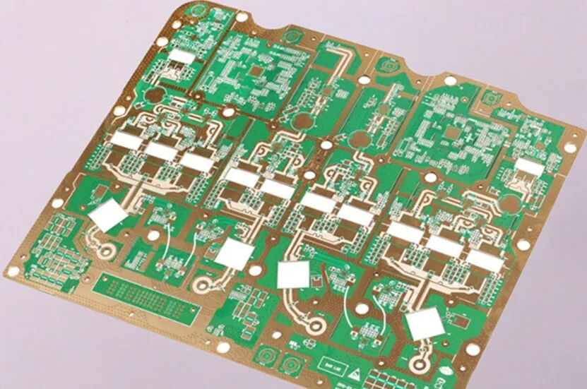
High-Frequency and High-Speed Boards
Made from high-performance materials such as polyimide (PI) or polytetrafluoroethylene (PTFE), characterized by low dielectric loss, low signal delay, and high heat resistance, widely used in 5G communication, millimeter-wave radar, wireless transmission, RF modules, and other high-frequency and high-speed scenarios.
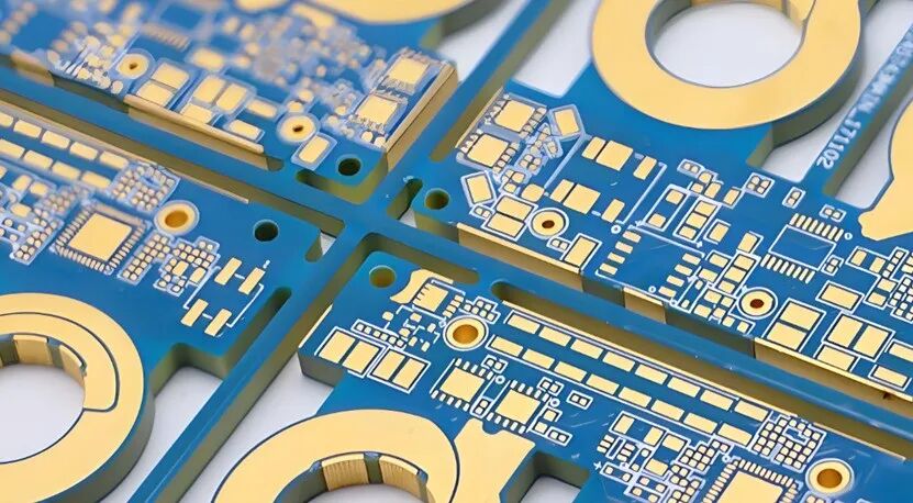
Heavy Copper Board (Heavy Copper PCB)
Has a copper foil thickness far exceeding that of conventional PCBs, suitable for large current and high power applications, such as power modules, motor drivers, inverters, etc.
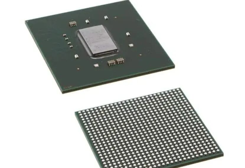
IC Packaging Substrate is a high-precision substrate used for chip packaging, featuring high-density wiring capabilities and high reliability, commonly found in advanced packaging technologies (such as FCBGA, WLP).
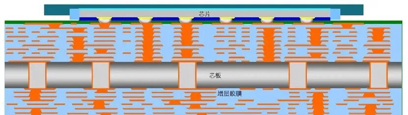
There are various classification methods for Printed Circuit Boards (PCBs), reflecting their diversity in materials, structures, processes, and application scenarios. With the continuous development of electronic technology, PCBs are evolving towards higher density, higher performance, thinner, and more reliable directions, becoming an important foundation supporting the intelligence and high performance of modern electronic devices.
5 Classification by resin system
Phenolic resin (such as FR-1, FR-2, XPc, etc.) is low-cost with poor flame retardancy, mainly used for low-end paper-based boards like 94HB.
Epoxy resin (such as FR-4, FR-5) has good mechanical properties and heat resistance, making it the most mainstream material for glass fiber cloth-based copper clad laminates.
Polyester resin is used in flexible circuits or special environments.
Special resins
Bis-maleimide triazine resin (BT): High frequency, low thermal expansion, used for packaging substrates.
Polyimide resin (PI): High temperature resistant, used for flexible circuit boards.
Polyphenylene oxide resin (PPO): Low dielectric constant, used in high-frequency and high-speed fields.
Maleic anhydride imide-styrene resin (MS), cyanate resin, polyolefin resin, etc.: Used for high-frequency and high-reliability products.
6 Classification by flame retardancy
Flame retardant type (UL94-V0, UL94-V1): Has good flame retardant properties, meeting safety standards.
Non-flame retardant type (UL94-HB): Poor flame retardant properties, mostly used for low-cost products.
In recent years, with the increase in environmental protection requirements, “green flame retardant CCL” has emerged, which is an environmentally friendly copper clad laminate without brominated flame retardants, meeting RoHS and other environmental directives.
7 PCB material brands and quality grades (from low to high)
Common PCB materials are ranked from low to high in quality and performance as follows:
94HB: Ordinary paper-based board, non-flame retardant, lowest-end material, cannot be used for power boards.
94V0: Flame retardant paper-based board, can be punched.
22F: Single-sided semi-glass fiber board, can be punched.
CEM-1: Single-sided glass fiber board, requires computer drilling, cannot be punched.
CEM-3: Double-sided semi-glass fiber board, suitable for simple double-sided boards, priced about 5~10 yuan per square meter cheaper than FR-4.
FR-4: Double-sided glass fiber epoxy resin board, with excellent overall performance, widely used.
8 Thickness specifications of prepreg
Prepreg is an important material used to bond various layers during the lamination process of multilayer boards, and its thickness directly affects the quality of interlayer bonding and electrical performance.
|
Model |
Thickness (mm) |
|
1080 |
0.0712 |
|
2116 |
0.1143 |
|
7628 |
0.1778 |
9 Dielectric constant of PCB materials (Dk / εr)
Definition of dielectric constant
The dielectric constant (Relative Permittivity, abbreviated as Dk or εr) is a physical quantity that describes the ability of a dielectric material to store electrical energy under the influence of an electric field. It is defined as:
Relative Dielectric Constant = Electric Field Strength in the Dielectric / Electric Field Strength in Vacuum
It is closely related to factors such as material polarity, frequency, temperature, and humidity.
Greater than 3.6: Strongly polar materials
2.8 ~ 3.6: Weakly polar materials
Less than 2.8: Non-polar materials
The dielectric constant affects signal transmission
The dielectric constant directly affects the propagation speed of electrical signals in PCBs, with the relationship being:
Signal Propagation Speed ∝ 1 / √Dk
That is: the lower the dielectric constant, the faster the signal propagation.
For example: Running on the beach, the “viscosity” of the water is like the dielectric constant; the stickier the water (the higher the Dk), the slower you run.
10 Key parameters of FR4 materials
Dielectric constant (Dk)
The Dk of FR4 is typically between 4.0~4.5, with specific values varying by brand and testing conditions.
For example: Shengyi FR4 has a Dk of about 3.7, while Ultrasonic FR4 is about 4.2.
Dielectric loss (Df / Loss Tangent)
Indicates the degree of energy loss of the material under an alternating electric field, usually represented by tanδ or Df.
The Df of FR4 is generally around 0.02, increasing with frequency.
Glass transition temperature (Tg)
Tg is the temperature at which the material transitions from a glassy state to a rubbery state, an important indicator of the board’s heat resistance.
Common FR4 Tg values include: 130℃, 140℃, 150℃, 170℃, etc. The higher the Tg, the better the heat resistance.
Common thickness range: 0.3mm ~ 2.0mm
Thickness tolerance is determined by the manufacturer’s process.
11 Copper foil thickness
Common copper foil thicknesses: 0.5 oz, 1 oz, 2 oz (1 oz ≈ 35 μm)
Special requirements can customize thicker copper foil.
Relationship between prepreg and FR4 materials
FR4 is a copper clad laminate made with glass fiber cloth as the reinforcing material and epoxy resin as the matrix.
CEM-3 is a composite substrate, intermediate between paper-based and glass fiber cloth-based, with slightly lower performance than FR4, but at a lower cost.
Prepreg plays a bonding role in multilayer board lamination, and its models (such as 1080, 2116, 7628) correspond to different thicknesses and resin content.
The dielectric constant of PCB substrate materials is one of the core parameters affecting signal integrity, transmission speed, and electromagnetic compatibility. As electronic products evolve towards high frequency, high speed, and high density, the demand for high-performance boards with low Dk, low Df, and high Tg is increasing. Engineers should consider various factors such as product application scenarios, frequency characteristics, and cost budgets when selecting PCB materials to ensure product performance and reliability.
Basic structure of Printed Circuit Boards (PCBs)
1 Overall Structure
A Printed Circuit Board (Printed Circuit Board, PCB) is a substrate used to support and connect electronic components, and its basic structure consists of multiple material layers bonded together through a thermal pressing process.PCBs typically adopt an even-layer structure, with symmetrical distribution of layer thicknesses to ensure electrical performance and structural stability. The four main materials that constitute the circuit loop include: copper foil, core material, prepreg (Prepreg), and solder mask.
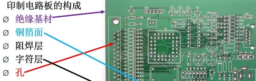
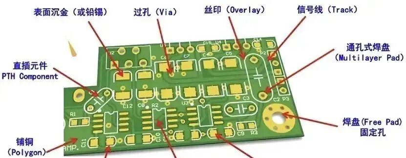
The following is an example of the most basic 4 layer PCB structure, illustrating its composition: This structure consists of a core board (Core) and two prepreg layers (Prepreg) combined through a thermal pressing process.

2 Internal Structure (Stacked Structure)
The stacked structure of a PCB is the core part of its design and manufacturing, and the selection and combination of materials for each layer directly affect the performance and cost of the circuit.
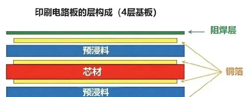
Below is a detailed description of the materials for each layer:
Copper Foil (Copper Foil) — Conductive Layer
Copper foil is the key material in PCBs for achieving signal transmission and current conduction, with good conductivity and processability. In conventional PCBs, the thickness of copper foil is usually 35μm (1oz), but in high current or high power applications, thicker copper foil can be used, such as 70μm (2oz) or higher.
The thickness of copper foil is usually expressed in ounces (oz), where 1oz is defined as: spreading 1 ounce (28.35g) of copper foil evenly over an area of 1 square foot (929cm²), resulting in a copper foil thickness of about 1.37mil (approximately 35μm). Common copper foil thickness specifications include: 12μm (1/3oz), 18μm (1/2oz), 35μm (1oz), 70μm (2oz).
Core Material (Core) — Insulating Layer
The core material is the insulating material that forms the basic structure of the PCB, primarily serving to achieve interlayer insulation and provide structural support. The core material is usually made from glass fiber cloth and epoxy resin, and its material selection directly affects the PCB‘s electrical performance, thermal stability, and cost. Therefore, the selection of core material should be optimized based on the specific requirements of the circuit design.
Prepreg (Prepreg) — Bonding Layer
Prepreg is the bonding material in the stacked structure of PCBs, primarily providing interlayer insulation and bonding functions. Prepreg is made from glass fiber cloth impregnated with epoxy resin, which softens when heated and exerts adhesive effects, achieving thermal lamination of multilayer structures.
The basic manufacturing process is as follows:
Melted glass slurry → Glass fibers → Glass yarn → Glass cloth (Glass Fiber)
Glass cloth + Epoxy resin (Epoxy) → Prepreg (Prepreg)
Prepreg + Copper foil → Copper Clad Laminate (CCL),
Copper Clad Laminate (CCL) is the basic material for PCB manufacturing, commonly referred to as “board material”. In multilayer board manufacturing, CCL is also referred to as “core board” (Core).
Solder Mask (Solder Mask) — Surface Protection Layer
The solder mask is an insulating protective layer coated on the surface of the PCB to prevent copper foil oxidation, short circuits, and improve circuit stability. The solder mask is commonly referred to as “windowing” to expose pads for soldering operations. The solder mask is divided into a top layer (Top Solder) and a bottom layer (Bottom Solder).
Although green is the most common color for PCBs, other colors such as red, blue, yellow, black, and white can also be selected based on design requirements.
3 Classification and functions of PCB layers
In PCB design, different functional layers are used to achieve circuit wiring, protection, identification, and manufacturing requirements.
Generally, companies will define and classify each layer based on their actual situation during the design process, and this will be integrated into their entire business activities, including procurement, inventory management, production, and sales. In procurement and sales, engineers will also generate a classification correspondence table with suppliers and customers based on their classifications to unify the naming conventions or part number rules between different suppliers and customers. Of course, you can also refer to the following image:
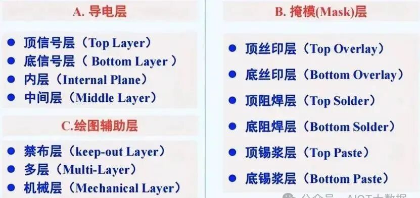
Below are common classifications of PCB layers and their functional descriptions:
Signal Layers
Top Layer (Top Layer) and Bottom Layer (Bottom Layer): Used for wiring and component placement, they are the most basic conductive layers in PCBs.
Mechanical Layers
Mechanical Layer: Used to define the external dimensions of the PCB, mounting hole positions, and other mechanical structure information, without electrical properties. Typically, up to 16 mechanical layers can be set.
Silkscreen Layers
Top Overlay (Top Overlay) and Bottom Overlay (Bottom Overlay): Used to identify component numbers, annotations, LOGO, and other assembly information, usually in white, using silk screen printing technology.
Paste Layers
Top Paste (Top Paste) and Bottom Paste (Bottom Paste): Used to indicate the pad positions that need to be coated with solder paste in the SMT (Surface Mount Technology) process, which is a key layer for surface soldering.
Drill Layers
Drill Grid (Drill Grid) and Drill Drawing (Drill Drawing): Used to provide drilling information during the PCB manufacturing process, including the drilling positions and sizes of vias, pads, etc.
Keep Out Layer
Used to define the boundaries, slots, and cutouts of the PCB, restricting the placement range of wires and components to ensure the integrity and safety of the circuit design.
Multi Layer
Multi Layer is an abstract layer used to represent the electrical connection paths of components (such as through-hole pads, vias, etc.) that need to span the entire PCB. The graphics on this layer will be reflected in all conductive layers (except for plane layers), typically used to define plated holes (PTH) or non-plated holes (NPTH).
Through the systematic description of the above structures and functions, clear technical basis and engineering guidance can be provided for the design, manufacturing, and application of PCBs.
Below is a comparison diagram of customer and factory PCB descriptions:
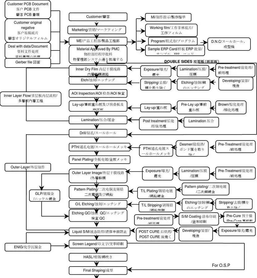
PCB Manufacturing Process Flow
The manufacturing process of Printed Circuit Boards (PCBs) can be systematically divided into three core stages: inner layer production, outer layer production, and packaging molding, with each stage achieving the transformation from substrate to finished product through precise process control. The specific process analysis is as follows:
1 Inner Layer Production: Building the Circuit Base Layer
As the core foundation of the multilayer structure of PCBs, inner layer production achieves high-precision circuit pattern transfer and interlayer stacking through the following refined processes:
Substrate Preparation: Select a substrate material that meets electrical performance requirements (such as FR-4 epoxy resin glass fiber cloth substrate) as the physical medium for circuit support.
Copper Layer Pattern Etching: Using photolithography, cover the substrate surface with a photosensitive dry film, transfer the designed circuit pattern to the dry film through exposure and development, and then precisely remove excess copper layers through chemical etching to form the target circuit pattern.
Interlayer Alignment and Stacking: High-precision alignment of multiple etched copper-clad boards and prepreg sheets (PP) is performed in a vacuum hot press, where controlled temperature (usually 150-180℃), pressure (about 30-50kg/cm²), and time (60-90 minutes) work together to achieve resin melting and bonding between layers, forming a stable multilayer stack structure.
Edge Trimming: Remove excess material from the edges of the laminated board using CNC milling to ensure dimensional accuracy of the laminated board, providing a flat reference surface for outer layer circuit production.
Technical Value: Inner layer production controls pattern transfer accuracy (±0.05mm) and interlayer alignment tolerance (≤0.075mm), providing a reliable electrical channel foundation for subsequent outer layer interconnections.
2 Outer Layer Production: Achieving Circuit Function Integration
Based on the inner layer substrate, outer layer production completes circuit function construction through pattern transfer and surface treatment:
Through-Hole Drilling: Using CNC drilling machines (precision ±0.02mm), drill conductive holes (PTH) and blind holes on the inner laminated board, with hole diameters ranging from 0.15-6.35mm, achieving interlayer electrical interconnection channels.
Hole Metallization: Through chemical copper deposition (PTH copper thickness ≥20μin) and electroplating thickening (copper thickness usually 18-35μm), a continuous conductive layer is formed on the hole walls to ensure current conduction between layers.
Pattern Transfer: Repeat the inner layer etching process, using LDI (Laser Direct Imaging) technology to achieve finer line width/spacing control (minimum 3/3mil), completing the outer layer circuit pattern production.
Surface Treatment: Select processes such as gold plating (ENIG), OSP (Organic Solderability Preservative), or hot air leveling (HASL) based on application needs to enhance pad solderability and oxidation resistance.
Reliability Verification: Conduct continuity testing using flying probe testing (Flying Probe), combined with thermal shock (-55℃~125℃ cycles), and damp heat (85℃/85%RH) environmental tests to ensure electrical performance and mechanical stability meet standards.
Process Breakthrough: The introduction of the AOI (Automated Optical Inspection) system in outer layer production allows for real-time interception of defects such as pad gaps and line breaks, improving yield to over 99.8%.
3 Packaging and Molding: Fine Processing of Finished Products
After completing the construction of electrical performance, the following steps are required to achieve product standardization and quality assurance:
Surface Marking Printing: Use silk screen printing or coding technology to mark silkscreen characters (component designations, polarity markings, etc.) on the board surface, with character heights of 0.8-2.0mm, complying with IPC-7351 standards.
Shape Processing: Use CNC milling machines or V-CUT dividing machines to cut large boards into specified shapes (such as rectangles, irregular shapes), with dimensional tolerances controlled within ±0.1mm and edge flatness ≤0.05mm.
Full Inspection Screening:
Electrical Performance Testing: Use flying probe testers or ICT online testers to conduct 100% continuity, insulation resistance, and withstand voltage tests on each PCB, ensuring no short circuit/open circuit defects.
Visual Full Inspection: Use high-resolution CCD visual systems to conduct 100% manual re-inspection of board surface scratches, contamination, character integrity, etc., with a defect rate controlled at ≤0.1%.
Packaging Specifications: Qualified products are vacuum-packed in anti-static packaging (humidity <10%RH), with each tray equipped with humidity indicator cards and desiccants to ensure that the transportation and storage environment meets EIA-481 standards.
The entire process in the factory workshop can refer to the following diagram:
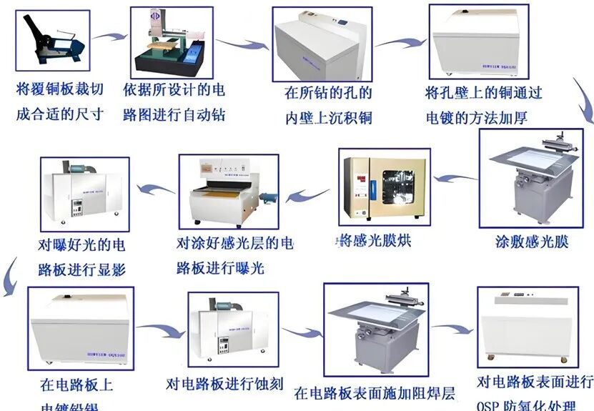
PCB manufacturing process reference diagram:
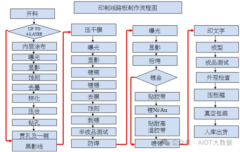
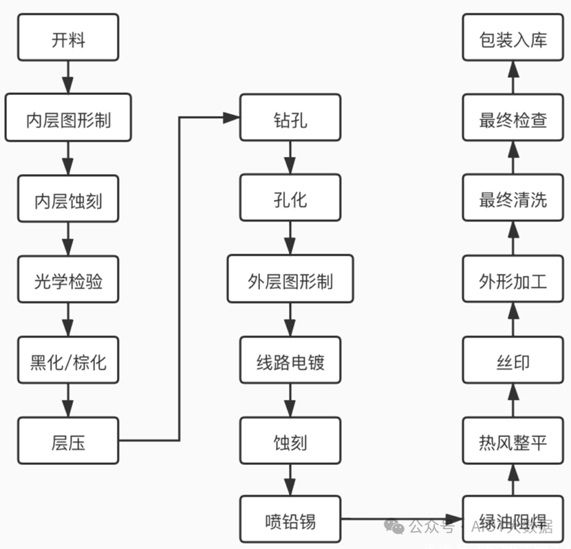
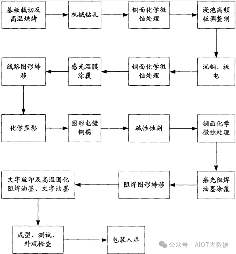
The differences in PCB manufacturing, aside from the differences in the number of layers, include significant distinctions between standard boards and high-frequency boards, mainly due to the special processing techniques addressing more dielectric influencing factors for high-frequency signals.
The process flow for standard boards is simplified as follows:
The process flow for high-frequency boards includes additional process references as follows:
Through the precise collaboration of the above process chain, PCB manufacturing ultimately achieves the transformation from substrate to high-reliability electronic carriers, meeting the stringent demands for high density and high reliability in consumer electronics, automotive electronics, communication equipment, and other fields.
The above content is reproduced from the internet. If there is any infringement or omission, please contact us in the background for correction or deletion!
—END—