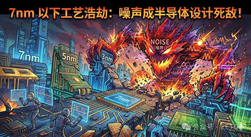
Noise has always been a core concern for communication experts, but it is now rapidly becoming a tricky problem that every semiconductor designer must face—— Some chips are already experiencing performance degradation issues.
Noise can be defined as any interference that deviates from the ideal state and may affect the expected functionality. In the semiconductor field, this means that it is impossible to reliably extract signal values at designated times, or the device voltage cannot maintain sufficient stability to ensure reliable signal generation and detection.
In the communication field, noise is typically analyzed through eye diagrams. These charts can visually present whether noise has invaded the critical area for reliable signal extraction. Noise includes two dimensions: amplitude noise and phase noise. Phase noise arises from timing variations in the signal (especially clock signals), while amplitude noise can also cause phase shifts in clock edges (i.e., jitter), thereby affecting timing performance.
The sources of noise injection are diverse. At the device level, the primary culprits are bias temperature instability (BTI) and flicker noise, but the currently more concerning noise sources have a destructive range that is an order of magnitude larger for chip design.
“As semiconductor process nodes break through 7nm, packaging technology becomes increasingly complex, and power distribution network (PDN) noise has become a core challenge,” said Mohammed Hassan, a 3D-IC solutions engineer at Siemens EDA. “Lower supply voltages, higher current densities, and denser interconnect structures lead to exacerbated IR drop, inductive noise (L・di/dt), and PDN discontinuity issues between stacked chips. If not properly managed, dynamic voltage noise can reach 5% to 10% of the nominal VDD.”
Noise management has become one of the most critical and persistent challenges in modern semiconductor design.“With power supply voltage dropping to around 1 volt and transistor density continuously increasing, the traditional design margins that could absorb electrical fluctuations have essentially disappeared,” said Charlene Wan, Vice President of Brand, Marketing, and Investor Relations at Ambiq. “Previously insignificant small fluctuations can now directly jeopardize chip performance or reliability.”
Power Integrity and Signal Integrity
Some issues, although not new, have fundamentally changed in their impact context.“Signal integrity has been studied at the system level for over 30 years,” said John Parker, Product Management Director at Cadence’s Custom IC and PCB division. “We have advanced 3D electromagnetic field solvers that can extract high-precision S-parameters of channels and model them. However, for chip designers, unless it involves analog circuit design, this concept may be extremely unfamiliar. Today, the traditional design boundaries between chip and system are accelerating towards integration.”
Currently, the power consumption of cutting-edge chips is exploding, leading to a series of chain problems.“Noise is an interference layer above digital design,” explained Marc Swinnen, Product Marketing Director at Ansys, a subsidiary of Synopsys. “Power lines should remain absolutely stable, but the actual fluctuations are power noise. The high-intensity burst working modes of digital modules severely affect power supply stability, while sensitive areas in analog or digital designs require even higher power stability, thus necessitating separate power lines.”
This design also gives rise to new problems.“Current complex SoCs typically contain 20 to 30 voltage domains, but only 2 to 3 of them are high current domains,” said Andy Heinig, Head of Efficient Electronics at the Fraunhofer Institute for Integrated Circuits. “The core voltage domain and 1 to 2 I/O voltage domains belong to high current domains, while the power consumption of the remaining 10 to 20 voltage domains is only in the microamp range, mainly used for standardized modules like phase-locked loops (PLLs), which must minimize their noise levels. However, advanced packaging technology makes all interconnect structures highly dense, exacerbating crosstalk issues. The key contradiction is not the absolute strength of the noise, but that the noise across all power networks (including critical domains) is increasing — the reduced interconnect spacing leads to intensified coupling effects, a trend that is unavoidable. Overall, increased noise and enhanced coupling are creating new challenges.”
The proliferation of advanced packaging technology has made some issues more pronounced.“In analog/mixed-signal designs such as DDR physical layers (PHY) or high bandwidth memory (HBM) interfaces, the consequences of IR drop are particularly severe,” noted Takeo Tomine, Chief Product Manager at Ansys, a subsidiary of Synopsys. “For example, in DDR interfaces, local IR drops at terminals or driver circuits can lead to signal swing attenuation, causing eye diagram closure and bit errors; in HBM designs, when multiple high-speed I/O channels operate in parallel, even minor voltage drops can disrupt timing margins, leading to data corruption or synchronization failures.”
Other system-level issues are gradually migrating into the package.“Like multi-component systems on PCB boards, when one chip starts up and another chip goes to sleep and then switches back to the former, it can cause power oscillations,” said Swinnen from Ansys. “The power distribution network has resonant frequencies, and if the frequency of power consumption changes matches it, oscillation amplification occurs. Such low-frequency oscillations have never occurred in single-chip devices.”
As package sizes increase, these problems become more complex.“When traces on the interposer extend to other chips, the impact of inductance (L) dramatically amplifies,” said Joe Davis, Senior Director of Product Management at Siemens Digital Industries Software. “Resonance phenomena are inevitable, and 3D-ICs are beginning to face traditional packaging’s signal integrity issues. Although the interconnect lengths are shorter than wires, the current foundry technology roadmap indicates that integrated systems containing hundreds of chips will emerge in the future, at which point the effects of inductance and capacitance (C) will become critical factors.”
It is not just data center chips that are affected.“For ultra-low-power chips operating at near-threshold voltages (such as wearable devices and IoT edge devices), noise issues are further amplified,” said Wan from Ambiq. “These SoCs sacrifice voltage margins for energy efficiency, making them inherently more sensitive to voltage drops, jitter, and crosstalk.”
Multi-Physics Collaborative Challenges
Multi-physics issues have become the norm in the industry.“From a packaging perspective, advanced platforms such as 2.5D/3D integration, fan-out packaging, and redistribution layer interposers bring new challenges,” said Rosalia Beca, Chief Technology Officer at Rapidus Design Solutions. “Analog modules are easily affected by power integrity issues, thermal gradients, and inter-chip crosstalk, all of which can lead to performance degradation. System-in-package (SiP) integrates RF, analog, and digital components, making verification work more complex, requiring multi-physics simulations covering electromagnetic interference, thermal behavior, and signal integrity.”
New problems are emerging in the field of electromagnetic coupling.“Noise issues in digital systems are relatively simpler than in microwave or RF systems,” said Niles Kandar, General Manager of Design and Verification at Keysight Technologies. “However, as frequencies continue to rise, everything can become a noise source — any component or connection can have positive or negative effects. In high-frequency environments, even small structures of packages or connections can become antennas, and if not designed properly, signal leakage can interfere with adjacent chips.”
This trend has long been anticipated.Mo Faisal, CEO of Movellus, predicted seven years ago: “By laying wires directly on the chip surface and connecting them to an oscilloscope, noise synchronized with the switching frequency can be observed. Since wires can detect it, 3D chip stacking will naturally be affected. This is a system-level issue that must be addressed by spreading noise frequencies through techniques like spread spectrum to avoid concentrated interference. Electromagnetic radiation between chips is inevitable, and spread spectrum technology can effectively reduce interference risks.”
Some mechanisms of these problems have only recently been deeply understood.“We cannot assume that complex chips or packaging systems at 5G or 6G levels will work normally based solely on past experience,” said Kandar from Keysight Technologies. “We are entering the deep waters of multi-physics issues — electromagnetic effects, power leakage, and thermal effects intertwine and influence each other. For example, high temperatures can change electromagnetic characteristics, while high power consumption can trigger thermal shocks, all of which are detrimental to design. In the past, the distances between system components were large, and interactions were weak, making these issues negligible, but now we must confront them head-on. With the development of heterogeneous integration and millimeter-wave technologies, collaborative management of multi-physics has become a new industry challenge.”
Some new effects are exacerbating existing problems.“As customer frequency requirements increase, the demand for modeling accuracy of clock jitter and clock uncertainty is also rising,” said Manoj Palaparthi, Senior Staff Product Manager at Synopsys. “These effects have always existed, and designers typically leave margins to cope, but now aging issues are drawing attention, requiring consideration of both the chip’s new state and the clock jitter characteristics after aging. How will the clock structure perform in two years? Will duty cycle distortion worsen? Will jitter change? These all need precise predictions.”
Noise Analysis and Verification Challenges
Noise is increasingly burdening verification work.“Circuits like HBM deeply intertwine analog and digital domains, significantly increasing the scope and importance of verification work,” said Karthik Koneru, Chief Product Manager at Synopsys. “Regression test suites now contain thousands of tests, requiring not only functional correctness but also high precision under process corners, noise conditions, and timing scenarios. The core challenge is to achieve the accuracy of analog verification without sacrificing the speed of digital-level regression testing.”
The actual impact of noise is already significant.“SoCs containing analog/mixed-signal (AMS) modules typically have a first silicon success rate that is 10% to 15% lower than pure digital chips,” said Beca from Rapidus. “This gap mainly arises from insufficient boundary scenario coverage, inadequate modeling, and integration issues such as power domain conflicts and substrate noise.”
Analysis methods can combine static and dynamic IR drop simulations, electro-thermal PDN modeling, and on-chip voltage sensors to capture transient drops and resonant behaviors across different frequency ranges. “Noise suppression can be implemented at the chip, package, or circuit board level,” said Hassan from Siemens. “At the chip level, wider power lines, more vias, decoupling capacitors, and global optimization strategies such as current sensing layout planning and adaptive voltage regulation can be employed; at the package or circuit board level, layered decoupling (chip, package, PCB), low-inductance power/ground planes, optimized PDN impedance, and efficient voltage regulators (VRM) placed near loads can be utilized.”
The importance of model verification has significantly increased.“I see the industry investing a lot of time and effort in model verification; if this step is missing, the entire design foundation will collapse,” said Satish Balasubramaniam, Head of AMS Product Management and Marketing at Siemens. “During verification, it may suddenly be discovered that the clock jitter of the PLL far exceeds expectations or that the target clock signal cannot be generated, with many subtle issues involved. Model verification has become a major pain point in the industry.”
Perhaps the most severe problem is that many noise faults are silent data errors—— the root cause is difficult to locate and very hard to reproduce. “In low-power devices, these faults may not manifest as system crashes,” said Wan. “Instead, they may reflect as reliability drift, sensor count errors, Bluetooth packet loss, or shortened battery life due to additional power consumption.”
Impact on Team Collaboration
These are not just technical issues; they also bring challenges at the organizational collaboration level.“We need to redefine acceptable noise thresholds,” said Heinig from Fraunhofer. “With the proliferation of chiplets and advanced packaging, related questions will continue to increase. On the power side, more simulations are needed to avoid IR drops under different workloads — this is a big issue because high integration of components leads to domain overlap. Engineers are accustomed to dividing designs into different domains, with power domains having their own models and solutions, but now, with increased interactions between components, engineers are required to collaborate across domains, and they often lack a common technical language.”
All practitioners need to learn new skills.“As a digital IC designer, I never thought I would need to analyze problems using 3D electromagnetic field solvers,” said Parker from Cadence. “But now it is essential to master. Similarly, packaging designers previously did not need to pay attention to formal design rule checks (DRC), but this has also become a necessary skill. This is a process of integrating system design with chip design tools and expertise. Designers in analog or RF fields are very familiar with electromagnetics, while our core work is to integrate these processes so that engineers can use the required tools smoothly without crossing technical gaps.”
Potential Solutions
Existing tools can achieve noise management.“Front-end design can indirectly influence noise at the RTL level, such as through activity balancing, clock gating, and power domain control,” said William Wang, CEO of ChipAgents. “However, the key to reducing IR drop and power integrity noise lies in back-end design — power grid layout, decoupling strategies, and packaging planning determine actual noise performance. In the future, AI agents are expected to play an important role in back-end optimization: autonomously analyzing electromagnetic/IR simulation data, learning from past sign-off data, and proposing optimization suggestions for layout or decoupling capacitor placement to reduce voltage drop hotspots and improve power distribution efficiency at the chip and package levels.”
As problems intensify, the industry is investing more resources in researching long-term solutions. The widespread application of on-chip voltage regulators is one of the key considerations.“The bottleneck of integrated voltage regulators lies in developing magnetic components that can be integrated within the package,” said Luca Vassalli, Director of Customer Applications Engineering at Empower Semiconductor. “Switching regulators require inductance to work efficiently, and these inductors need to have energy storage capabilities and be as efficient as possible to avoid excessive power consumption. To achieve miniaturization, the switching frequency of the converters must be increased while maintaining high efficiency at small sizes.”
However, this solution also has drawbacks.“This means additional chip area is required, which in turn increases costs,” said Heinig. “Currently, through reasonable packaging design and the use of isolation and shielding techniques, it is possible to avoid critical power domains from being disturbed by noise from other signals, so it is not yet essential. However, on-chip voltage regulators may simplify complex simulations — even if the power network introduces noise, after internal regulation, critical modules like PLLs can still receive noise-free power. This could be an alternative to complex simulation techniques: the traditional method is to avoid power noise, while the new approach eliminates noise through internal filtering. However, companies typically only adopt new solutions when absolutely necessary, as initial implementation can bring uncertainty and potentially cause other issues.”
Unfortunately, the fundamental solution still lies in strengthening engineering specifications.“No design can completely eliminate noise, but through careful architectural design and implementation, noise can be effectively suppressed,” said Wan. “The design philosophy is crucial — treating the chip, package, and system as an integrated PDN design challenge to create low-noise chips from the source. The trends of heterogeneous integration, high-density packaging, and near-threshold computing will only exacerbate and complicate noise issues. For ultra-low-power systems, effective noise management can extend battery life by weeks or even months.”
Original article:
https://semiengineering.com/noise-a-chip-killer
Welcome to join the EETOP WeChat group
Registration for AMD Technology Summit: FPGA/SoC+x86 Embedded