Disclaimer: The images in this article are sourced from the internet. Please contact us for removal if there are any copyright issues.
Why can the CPU control hardware so precisely? The secret lies in memory mapping! It assigns a unique address “house number” to all components in the chip, such as memory and peripherals. The CPU can then accurately command everything by following this map, simplifying complex hardware interactions into simple memory read and write operations. By understanding this “urban planning” system, you grasp the underlying logic of embedded development.
The microcontroller system accesses all peripherals, code memory, data memory, and other modules through their positions in memory (memory addresses).
Memory mapping essentially allocates an address range for each different module in the microcontroller system, allowing the core processor to interact with these modules by referencing their addresses.
Memory mapping enables the processor to efficiently retrieve or send data from specific locations in the microcontroller space. For example, if the processor needs to retrieve sensor data from an Analog-to-Digital Converter (ADC), it must reference the address range specified for this ADC, and the ADC module will transmit the data upon receiving the signal.
Thus, memory mapping simplifies software development tasks, allowing developers to directly access and control peripherals as if they were ordinary memory addresses.
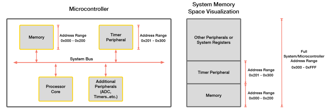
Memory addresses are typically referenced in hexadecimal, prefixed with 0x, followed by the hexadecimal address number.
How does the processor core read the next instruction to execute from code memory?
Looking at the memory mapping example above, if the processor wants to read data from memory, it simply needs to send a “read request” signal to a specific address within the range of 0x000 to 0x200 (for example, 0x100). When the memory device hears its address being called, it will immediately send the data at that address back to the processor via the bus.
How does the processor core write data to a timer peripheral’s register?
Similar to the reading process, the processor core needs to send data to an address within the range of 0x201 – 0x300 (for example, 0x22F). When the timer peripheral recognizes that it has been addressed, it immediately reads the data from the system bus and writes it into its local memory (such as a register).
It is important to emphasize one point, which is a common mistake for beginners: Each chip model has a different memory mapping. Do not assume that the address for chip A can be used for chip B. Therefore, before programming, always refer to the official datasheet or reference manual to find this “map”; otherwise, your program may not run.
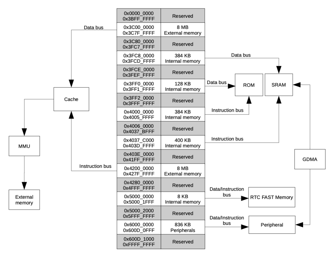
The ESP32-C3 follows the Harvard architecture, as it has separate data and instruction buses.
1. ROM (Flash Memory) addresses are mapped to two ranges:
-
Data bus: Memory address mapping range from
<span>0x3FF0_0000</span>to<span>0x3FF1_FFFF</span> -
Instruction bus: Memory address mapping range from
<span>0x4037_C000</span>to<span>0x403D_FFFF</span>
Both are internal storage and are within the same device package.
2. RAM addresses are mapped to two ranges:
-
Data bus: Memory address mapping range from
<span>0x3FC8_0000</span>to<span>0x3FCD_FFFF</span> -
Instruction bus: Memory address mapping range from
<span>0x4037_C000</span>to<span>0x403D_FFFF</span>
These are also internal storage.
3. Peripherals
Addresses are mapped to the range from <span>0x6000_0000</span> to <span>0x600D_0FFF</span>, which is used to access the registers or memory of peripherals.
Let’s illustrate the memory mapping process with a vivid example:

Imagine the microcontroller as a city, with the CPU as the mayor.
-
The city has residential areas (memory), timer offices, GPIO management offices, and various other departments (peripherals).
-
Memory mapping is like urban planning, assigning a unique address to each building in the city (for example, 1 Changshi Road is memory, and 20 Yuxin Road is the timer).
-
When the mayor (CPU) wants to read information from or issue commands to a department (peripheral), he does not need to know what the department looks like; he simply sends a letter (read/write request) to its address through the city’s communication system (system bus).
-
For example, the mayor sends a
<span>write</span>letter to address<span>0x22f</span>(a certain office in the timer office) with the content “Set the timer to 10 seconds”; the timer office will execute this operation upon receiving the letter.
The idea of treating everything as a memory address is the cornerstone of low-level embedded programming. In Rust’s low-level libraries (such as <span>PAC</span>), these complex address conversions are encapsulated into user-friendly functions, and understanding the underlying principles helps in better troubleshooting.
💡 Terminology and Concept Analysis (Key Concepts)
- Memory Mapping:
What is referred to as ‘memory mapping’ is better understood as a kind of ‘agreement’ or ‘protocol’. It specifies which address in the microcontroller corresponds to which functional component. With this agreement, the CPU does not need to care about what the specific hardware looks like; it can interact with the hardware simply by reading and writing to specific addresses.
- Address:
The ‘address’ here is analogous to a house number. It is essentially a unique identifier for each storage location in memory. The CPU uses this identifier to find the data it wants to operate on, precisely at that location.
- Address Range:
The address range refers to a segment of contiguous addresses allocated to a certain component. For example, memory may occupy addresses from <span>0x000</span> to <span>0x200</span>, while the timer occupies <span>0x201</span> to <span>0x300</span>.
- Hexadecimal:
This is a common counting method used in computers, represented by <span>0-9</span> and <span>A-F</span>. In code and documentation, it is usually prefixed with <span>0x</span>, for example, <span>0x100</span>.