1. Experimental Task
-
Task: Based on the STEP-MAX10M08 core board and STEP BaseBoard V4.0 baseboard, complete a simple voltmeter design and observe the debugging results.
-
Requirements: Measure the adjustable potentiometer output voltage through the serial ADC chip ADC and display the voltage information on the core board’s digital tube.
-
Analysis: Drive the serial ADC chip through FPGA programming to obtain the digitized voltage information, convert the quantized digital information into BCD code format, while driving an independent digital tube to display the voltage value.
2Experimental Purpose
In the basic digital circuit experiment section, we have mastered the principles and methods of FPGA driving independent digital tubes. This experiment mainly studies the related knowledge of the analog-to-digital converter ADC, the serial (SPI interface) ADC chip ADC081S101, and the driving design, while learning the design method of binary to BCD code conversion.
-
Learn the related knowledge of the analog-to-digital converter ADC.
-
Design the driving of the serial (SPI interface) ADC chip ADC081S101.
-
Learn the design method of binary to BCD code conversion.
-
Complete the design implementation of a simple voltmeter.
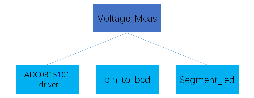
3Design Block Diagram
Based on the previous experimental analysis, we can conclude that this design can be divided into three functional modules:
-
ADC081S101_driver: Drive the SPI interface ADC chip to achieve analog voltage signal acquisition.
-
bin_to_bcd: Method to convert binary data into BCD code.
-
Segment_led: Display the voltage data through driving independent digital tubes.
Top-Down Hierarchical Design
Module Structure Design
4Experimental Principles
4ADC Introduction
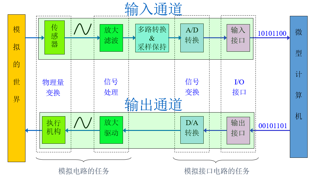
A digital system is a circuit that performs arithmetic and logical operations on digital quantities using digital signals, referred to as a digital circuit or digital system. However, the world we live in is analog, and to enable the digital system to help us process problems in our analog world, a bridge is needed to communicate between the digital and analog systems.
Model of the Combination of Analog and Digital Systems
An analog-to-digital converter, or A/D converter, commonly referred to as ADC, is an electronic component that converts an analog signal into a digital signal. A typical ADC converts an input voltage signal into an output digital signal. Since digital signals themselves do not have actual meaning and only represent a relative magnitude, any ADC requires a reference analog quantity as a standard for conversion, with the most common reference standard being the maximum convertible signal size. The output digital quantity represents the size of the input signal relative to the reference signal.
A digital-to-analog converter, also known as a D/A converter or DAC, is a device that converts digital quantities into analog signals. A DAC typically consists of four parts: a weighted resistor network, an operational amplifier, a reference power supply, and an analog switch. ADCs generally require DACs, as ADCs are devices that convert continuous analog signals into discrete digital signals.
As a bridge for converting between analog and digital systems, ADCs and DACs have many parameters to indicate their performance:
-
Resolution (Conversion Accuracy): Refers to the ratio of the minimum voltage to the maximum voltage that an ADC or DAC can collect or output, which is also the ratio of the minimum input digital quantity 1 to the maximum input digital quantity 2n-1. Resolution is usually expressed in terms of the number of bits of the digital quantity, typically 8 bits, 12 bits, 16 bits, etc. The resolution of an N-bit ADC or DAC is 2N.
-
Range (Full Scale Range, FSR): Refers to the range of analog voltage changes that an ADC or DAC can input or output.
-
Settling Time: Settling time is the time required for a DAC output to reach its final value, indicating the time from receiving the command to output until it settles within a certain accuracy range (usually 0.5 LSB, 1 LSB, 2 LSB).
-
Conversion Time: Refers to the time required for an ADC to obtain stable binary code from the moment the conversion command is issued. Conversion time is related to the type, principle, and bit number of the ADC.
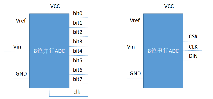
Parallel ADC and Serial ADC Models
Both of the above are 8-bit ADC models, with a resolution of 28 = 256, meaning that Vref is divided into 256 parts, and the resolvable analog step is Vref/256. The quantized data N = 256 * Vin/Vref.
-
Parallel ADC interfaces with digital circuits include one clk and 8 data pins. The clk is the chip clock pin, and the data pins collect 8 bits of data from the data pin in each clk cycle, completing one analog-to-digital conversion, so the clk frequency equals the sampling rate.
-
Serial ADC (taking ADC081S101 as an example) interfaces with digital circuits using three wires (cs, clk, din), compatible with the three-wire SPI bus. The cs is the chip enable pin, clk is the chip clock pin, and din is the chip data pin. When the ADC chip is enabled, each clk cycle collects 1 bit of data from din, but according to the timing of ADC081S101, 16 clks are needed to complete one sampling, so the clk frequency must be at least 16 times the sampling rate.
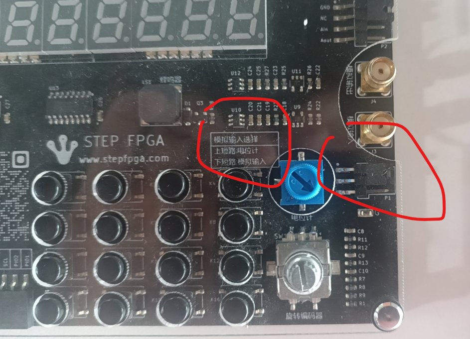
4.2 ADC Module Circuit Connection
Here we take the ADC module circuit on the STEP BaseBoard V4.0 as an example, with the circuit diagram as follows:
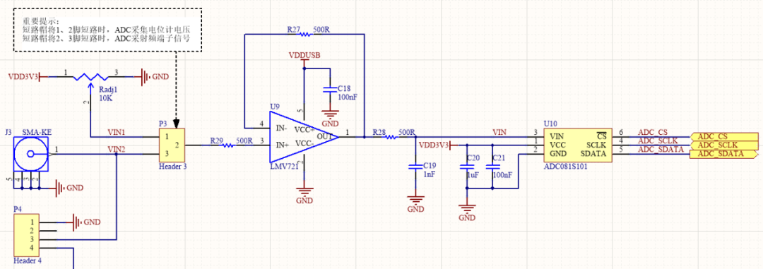
ADC Module Circuit
As shown in the ADC module circuit, the FPGA is directly connected to the control end of the ADC081S101 chip. The ADC has 6 pins, with pin 3 Vin being multiplexed for VCC and Vref, meaning Vin = VCC = Vref. The front end of the ADC is an operational amplifier circuit LMV721, with the op-amp module functioning as a voltage follower circuit. Further up is a jumper pin to select the source of the ADC sampling signal. When the jumper cap shorts pins 1 and 2, the ADC collects the potentiometer voltage; when the jumper cap shorts pins 2 and 3, the ADC samples the RF terminal or P4 pin signal. In this design, we are sampling the voltage of a rotary encoder, so we need to short pins 1 and 2 with the jumper cap.
4.3 ADC Module Driver Design
Previously, we learned that there are three wires (cs, clk, din) connecting the ADC081S101 chip and the PGA, compatible with the SPI bus. SPI stands for Serial Peripheral Interface, which is a high-speed, full-duplex, synchronous communication bus that occupies only four lines (cs, sck, mosi, miso) on the chip pins. In fact, three lines can also be used (for unidirectional transmission), which saves chip pins and PCB layout space. Due to this simplicity and ease of use, more and more chips are integrating this communication protocol.
SPI devices are divided into master and slave devices, sharing sck, mosi, and miso among devices. Additionally, each slave device has a cs line (not shared). Communication occurs between the master and slave devices, and slave devices cannot communicate directly with each other. The master can connect to multiple slaves simultaneously. When the master communicates with a specific slave, it first pulls the cs signal of that slave low, then transmits data through sck, mosi, and miso.
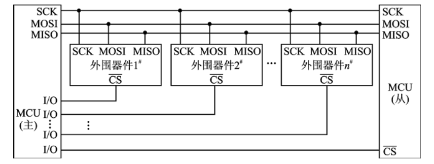
Multi-Device SPI Bus Connection
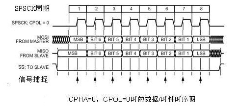
To make the SPI bus more flexible, it is divided into four modes controlled by two parameters:
-
CPOL: Clock Polarity Selection. When 0, SCK is idle at low level; when 1, SCK is idle at high level.
-
CPHA: Clock Phase Selection. When 0, sampling occurs on the first edge of SCK; when 1, sampling occurs on the second edge of SCK.
|
|
|
|
|
|
4 SPI Modes
The SPI bus protocol has four modes:
-
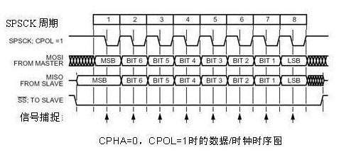
Mode 1: CPOL=0, CPHA=0: In this case, the idle state has SCLK at low level, and data sampling occurs on the first edge, which is the transition of SCLK from low to high, so data sampling occurs on the rising edge, and data is sent on the falling edge.
-
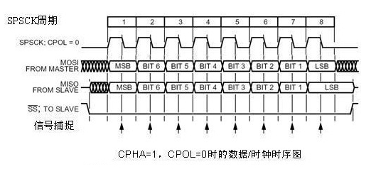
Mode 2: CPOL=0, CPHA=1: In this case, the idle state has SCLK at low level, and data is sent on the first edge, which is the transition of SCLK from low to high, so data sampling occurs on the falling edge, and data is sent on the rising edge.
-
Mode 3: CPOL=1, CPHA=0: In this case, the idle state has SCLK at high level, and data collection occurs on the first edge, which is the transition of SCLK from high to low, so data collection occurs on the falling edge, and data is sent on the rising edge.
-
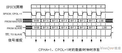
Mode 4: CPOL=1, CPHA=1: In this case, the idle state has SCLK at high level, and data is sent on the first edge, which is the transition of SCLK from high to low, so data collection occurs on the rising edge, and data is sent on the falling edge.
Pin Description Table for ADC081S101
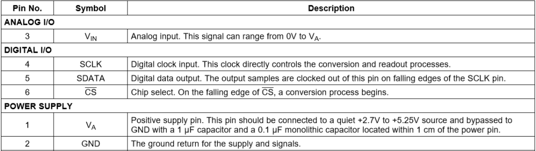
Note: The SDATA signal transmits data under the clock of SCLK. When SCLK is at the falling edge, SDATA updates the output data. When programming the driver, we need to sample data on the rising edge to obtain stable output.
The serial communication timing of ADC081S101 is shown in the following diagram:
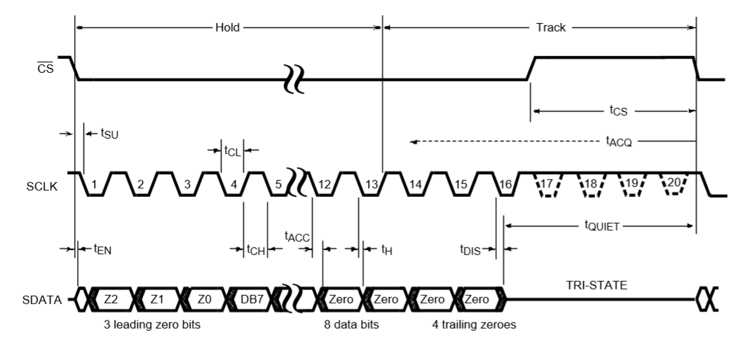
Note:
1. When SCLK is idle, it is at high level, CPOL = 1, sampling occurs on the rising edge (the second edge), and CPHA = 1. If the generic SPI core is instantiated, the fourth working mode of SPI must be used.
2. The CS signal is active low, and after 16 clocks, one ADC conversion and sampling is completed. The first three bits of the sampled data are invalid, followed by DB7~DB0 (valid data), followed by invalid data.
For the timing of ADC081S101, we use Verilog to design a counter that performs different operations based on the counter value, achieving one ADC sampling. The program implementation is as follows:
reg [7:0] cnt; // Counteralways @(posedge clk or negedge rst_n) if(!rst_n) cnt <= 1'b0; else if(cnt >= 8'd34) cnt <= 1'b0; else cnt <= cnt + 1'b1;reg [7:0] data; // Data as an intermediate buffer, output to the subsequent circuit after completing one ADC sampling, always @(posedge clk or negedge rst_n) if(!rst_n) begin adc_cs <= HIGH; adc_clk <= HIGH; end else case(cnt) 8'd0 : begin adc_cs <= HIGH; adc_clk <= HIGH; end 8'd1 : begin adc_cs <= LOW; adc_clk <= HIGH; end 8'd2,8'd4,8'd6,8'd8,8'd10,8'd12,8'd14,8'd16, 8'd18,8'd20,8'd22,8'd24,8'd26,8'd28,8'd30, 8'd32: begin adc_cs <= LOW; adc_clk <= LOW; end 8'd3 : begin adc_cs <= LOW; adc_clk <= HIGH; end //0 8'd5 : begin adc_cs <= LOW; adc_clk <= HIGH; end //1 8'd7 : begin adc_cs <= LOW; adc_clk <= HIGH; end //2 8'd9 : begin adc_cs <= LOW; adc_clk <= HIGH; data[7] <= adc_dat; end //3 8'd11 : begin adc_cs <= LOW; adc_clk <= HIGH; data[6] <= adc_dat; end //4 8'd13 : begin adc_cs <= LOW; adc_clk <= HIGH; data[5] <= adc_dat; end //5 8'd15 : begin adc_cs <= LOW; adc_clk <= HIGH; data[4] <= adc_dat; end //6 8'd17 : begin adc_cs <= LOW; adc_clk <= HIGH; data[3] <= adc_dat; end //7 8'd19 : begin adc_cs <= LOW; adc_clk <= HIGH; data[2] <= adc_dat; end //8 8'd21 : begin adc_cs <= LOW; adc_clk <= HIGH; data[1] <= adc_dat; end //9 8'd23 : begin adc_cs <= LOW; adc_clk <= HIGH; data[0] <= adc_dat; end //10 8'd25 : begin adc_cs <= LOW; adc_clk <= HIGH; adc_data <= data; end //11 8'd27 : begin adc_cs <= LOW; adc_clk <= HIGH; adc_done <= HIGH; end //12 8'd29 : begin adc_cs <= LOW; adc_clk <= HIGH; adc_done <= LOW; end //13 8'd31 : begin adc_cs <= LOW; adc_clk <= HIGH; end //14 8'd33 : begin adc_cs <= LOW; adc_clk <= HIGH; end //15 8'd34 : begin adc_cs <= HIGH; adc_clk <= HIGH; end default : begin adc_cs <= HIGH; adc_clk <= HIGH; end endcaseThus, we have completed the driver design for the serial ADC chip ADC081S101. The entire sampling cycle used 35 system clocks. If we use a 12 MHz clock as the system clock for this module, the sampling rate Fs = 12M/35 = 343K sps, and the ADC main frequency Fsclk = 12 MHz / 2 = 6 MHz.
The main frequency and sampling rate requirements for ADC081S101 are as follows. According to the requirements, our current main frequency and sampling rate are insufficient, so when using this module, a higher clock (such as 24 MHz) can be used to meet the chip’s requirements.
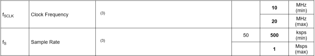
Note: The clock frequency Fsclk has a minimum value of 10 MHz and a maximum value of 20 MHz, with a sampling rate of 500 K sps to 1 M sps.
The module interface is as follows: clk and rst_n are the system clock and reset, adc_cs, adc_clk and adc_dat are the control pins for the ADC, adc_data is the ADC sampling data, and adc_done generates a pulse corresponding to the adc_data to obtain valid data.
input clk, // System clockinput rst_n, // System reset, active lowoutput reg adc_cs, // SPI bus CSoutput reg adc_clk, // SPI bus SCKinput adc_dat, // SPI bus SDAoutput reg adc_done, // ADC sampling complete flagoutput reg [7:0] adc_data // ADC sampling data4.4 Overall System Implementation
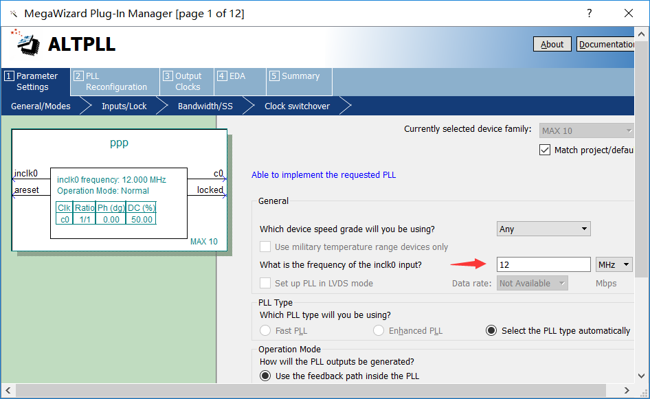
Due to the need for a higher clock for the ADC module, we instantiate a PLL core to obtain a 24 MHz clock. The method of instantiating PLL has been practiced in the basic digital circuit experiment section, so here we will briefly describe the process.
Open the IP Catalog tool under the Tools menu, find Library → Basic Functions → Clocks; PLLs and Resets → PLL → ALTPLL, open the ALTPLL configuration interface, set inclk0 input to 12 MHz, configure c0 clock output to 24 MHz, and leave all other options at default. Click Finish to complete the instantiation of the PLL core.
In the top-level module Voltage_Meas, instantiate both the PLL module and the ADC081S101_driver module, and connect the c0 output of the PLL to the clk of the ADC081S101_driver module.
The connection program for the PLL module and the ADC081S101_driver module is implemented as follows:
wire clk_24mhz, locked;pll u1(.areset (!rst_n ),// PLL module reset is active high.inclk0 (clk ),// 12MHz system clock input.c0 (clk_24mhz ),// 24MHz clock output.locked (locked )// PLL lock signal output);wire adc_done;wire [7:0] adc_data;// Use I2C bus to drive the ADC function of PCF8591, instantiate ADC081S101_driver u2(.clk (clk_24mhz ),// System clock.rst_n (rst_n ),// System reset, active low.adc_cs (adc_cs ),// SPI bus CS.adc_clk (adc_clk ),// SPI bus SCK.adc_dat (adc_dat ),// SPI bus SDA.adc_done (adc_done ),// ADC sampling complete flag.adc_data (adc_data )// ADC sampling data);Now we can obtain the ADC sampling data. Assuming the ADC analog input voltage is 3.3 V, theoretically, the sampled data we obtain should be 8’hff, and the final data displayed on the voltmeter should be 3.3. How do we convert 8’hff into a displayable 3.3 data? This involves the reverse calculation of the ADC quantized data. We know that the quantization operation is N= 256 * Vin/Vref, so the reverse operation is Vin = N * Vref/256, where Vref = 3.3V. Therefore, Vin = N * 0.0129, so we need to calculate the result of FPGA adc_data * 0.0129, and then to use decimal display, we first convert the result to BCD, and then display it on the digital tube.
Convert the ADC sampling data to voltage data according to the rules (multiply by 0.0129). Here we directly multiply by 129, and the data obtained after BCD conversion should have the decimal point shifted left by 4 bits. The program implementation is as follows:
wire [15:0] bin_code = adc_data * 16'd129;To convert the binary number into BCD code, we use the left shift and add three algorithm (taking 8’hff as an example):
(1) Left shift the binary code to be converted by 1 bit.
(2) After left shifting, the BCD code is placed in the hundreds, tens, and units.
(3) If the BCD code column after shifting is greater than or equal to 5, add 3 to that value.
(4) Continue the left shift process until all shifts are completed.
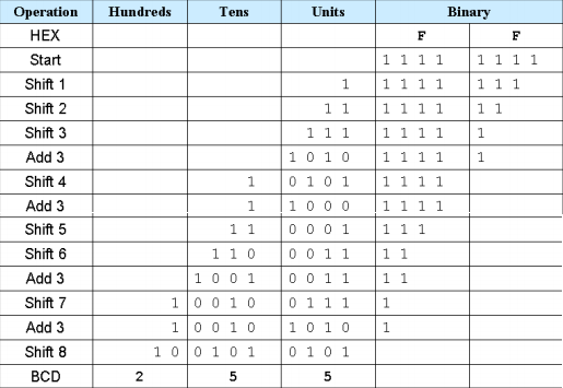
Binary to BCD code program implementation is as follows:
reg [35:0] shift_reg; always@(bin_code or rst_n)begin shift_reg = {20'h0, bin_code}; if(!rst_n) bcd_code = 0; else begin repeat(16) begin // Loop 16 times // BCD code each digit data performs full 5 add 3 operation, if (shift_reg[19:16] >= 5) shift_reg[19:16] = shift_reg[19:16] + 2'b11; if (shift_reg[23:20] >= 5) shift_reg[23:20] = shift_reg[23:20] + 2'b11; if (shift_reg[27:24] >= 5) shift_reg[27:24] = shift_reg[27:24] + 2'b11; if (shift_reg[31:28] >= 5) shift_reg[31:28] = shift_reg[31:28] + 2'b11; if (shift_reg[35:32] >= 5) shift_reg[35:32] = shift_reg[35:32] + 2'b11; shift_reg = shift_reg << 1; end bcd_code = shift_reg[35:16]; end endFinally, we obtain a 20-bit data output, with every 4 bits representing a BCD code, resulting in 5 valid data bits. Here we also need to shift the decimal point left by 4 bits, and the calculated number should be X.XXXX volts, with 1 integer bit and 4 decimal bits. The core board only has two digital tubes, so we take the highest two BCD codes to display on the digital tube as X.X volts, with the unit decimal point lit and the fractional decimal point off. The program implementation is as follows:
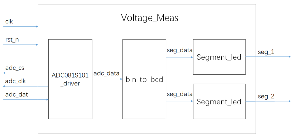
// Unit digital tube module instantiation Segment_led u4(.seg_dot (1'b1),// seg_dot input.seg_data (bcd_code[19:16]),// seg_data input.segment_led (seg_1 )// MSB~LSB = SEG,DP,G,F,E,D,C,B,A);// Fractional digital tube module instantiation Segment_led u5(.seg_dot (1'b0),// seg_dot input.seg_data (bcd_code[15:12]),// seg_data input.segment_led (seg_2 )// MSB~LSB = SEG,DP,G,F,E,D,C,B,A);The synthesized design block diagram is as follows:
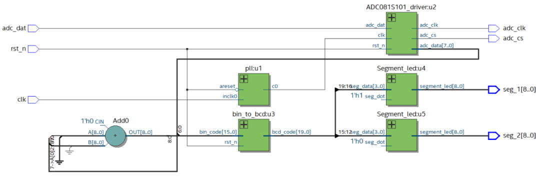
RTL Design Block Diagram
5Experimental Steps
(1) Double-click to open the Quartus Prime software;
(2) Create a new project: File→ New Project Wizard (name the project, select the project directory, select the device model, and EDA tool);
(3) Create a new file: File→ New→ Verilog HDL File, type the design code and save;
(4) Design synthesis: Double-click on the Analysis & Synthesis under the Tasks window to synthesize the code;
(5) Pin constraints: Assignments→ Assignment Editor, assign pins according to project requirements;
(6) Design compilation: Double-click on Compile Design under the Tasks window to compile the design and generate the configuration file;
(7) Program burning: Click on Tools → Programmer to open the configuration tool, and download the program;
(8) Observe the design running results.
6Experimental Phenomena
Download the program to the FPGA, use a jumper cap to short pins 1 and 2 on the P1 interface, rotate the potentiometer at the upper right corner of the baseboard, and observe the changes on the core board’s digital tube. If a multimeter is available, measure the voltage at the shorted P3 terminal and compare it with the digital tube display.