Without clicking the blue text, how can we have a story?Overview
This example mainly explains how to read and write the built-in Flash of the chip. Using the internal Flash of the chip can save some data that needs to be retained after power off, without the need to add external storage chips. This example uses the STM32F103RBT6 with a 128K Flash size.
QQ Group: 615061293
Sample Application
https://www.wjx.top/vm/ejaAT1c.aspx#
Generate Example
Use STM32CUBEMX to generate the example, here using the NUCLEO-F103RB development board.
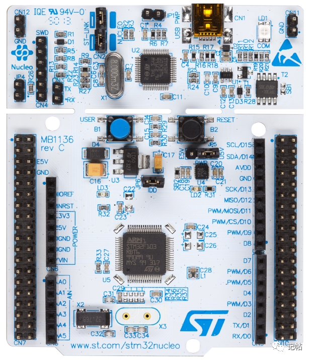
Check the schematic, PA2 and PA3 are set as the serial port of the development board.
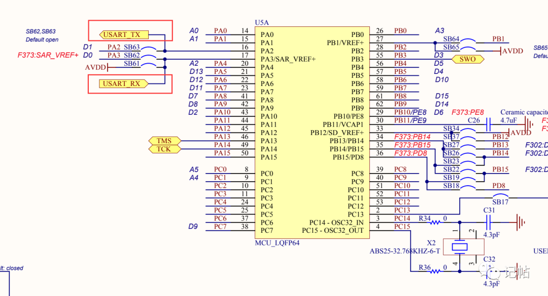
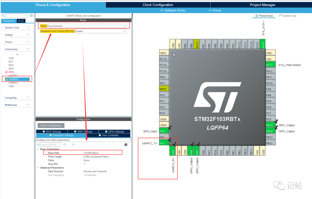
Configure the serial port.
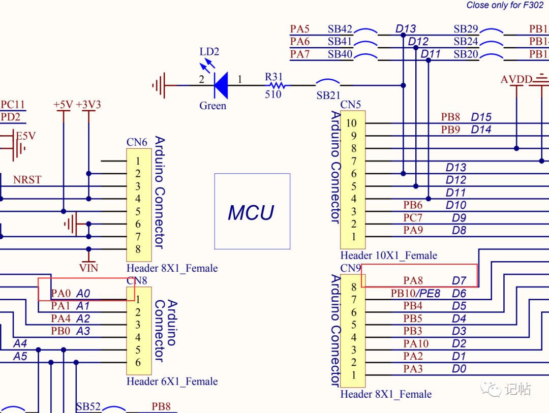
Check the schematic, PA8 is set as the PWM output pin, PA0 is set as the timer input capture pin.
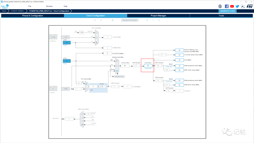
Configure Clock Tree
Configure the clock to 64M.
Redirect Serial Port
In main.c, add the header file. If not added, an identifier “FILE” is undefined error will occur.
/* USER CODE BEGIN Includes */#include "stdio.h"/* USER CODE END Includes */Function declaration and serial port redirection:
/* USER CODE BEGIN PFP *//* retarget the C library printf function to the USART */int fputc(int ch, FILE *f){ HAL_UART_Transmit(&huart2 , (uint8_t *)&ch, 1, 0xFFFF);return ch;}/* USER CODE END PFP */FLASH Definition
For STM32F103, there are low, medium, and high density FLASH types.
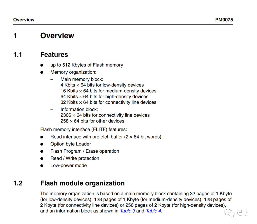
Low Density
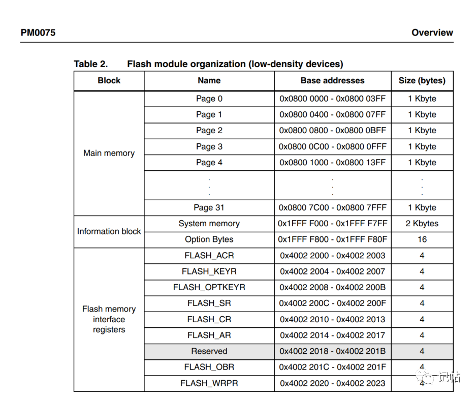
Medium Density
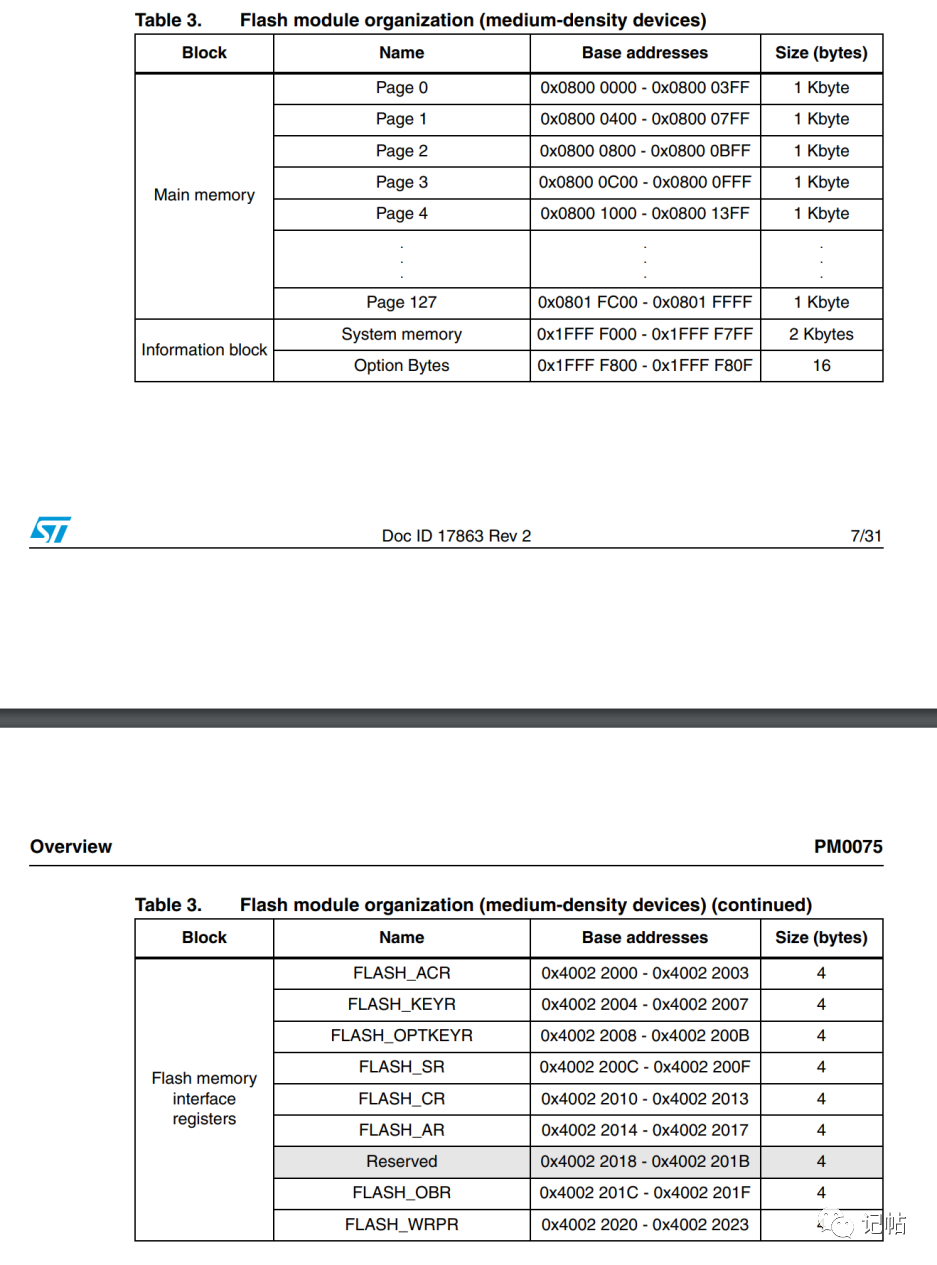
High Density
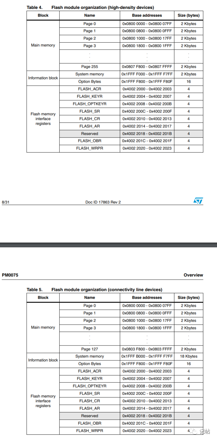
For STM32F103RB, the FLASH size is 128KB, which is classified as medium density Flash.
Variable Definition
/* USER CODE BEGIN 0 */uint32_t WriteFlashData[3] = {0x11111111,0x22222222,0x33333333};//Data uint32_t addr = 0x0801FC00;/* USER CODE END 0 */If you want to write data to FLASH, you need to perform the following four steps:
-
Unlock FLASH
-
Erase FLASH
-
Write to FLASH
-
Lock FLASH
Erasing can only be done by page or whole block.
The Flash capacity of STM32F103RBT6 is 128KB, so there are only 128 pages, each page is 1KB.
We can write to page 127, which is from 0x0801FC00 to 0x0801FFFF.
Since the microcontroller is 32-bit, when writing multiple uint32_t data continuously, the address should increase by 4 sequentially.
/* USER CODE BEGIN 4 *//*FLASH Write Program*/void WriteFlashTest(uint32_t L,uint32_t Data[],uint32_t addr){ uint32_t i=0; /* 1/4 Unlock FLASH*/ HAL_FLASH_Unlock(); /* 2/4 Erase FLASH*/ /*Initialize FLASH_EraseInitTypeDef*/ /*Erase method page erase FLASH_TYPEERASE_PAGES, block erase FLASH_TYPEERASE_MASSERASE*/ /*Erase page number*/ /*Erase address*/ FLASH_EraseInitTypeDef FlashSet; FlashSet.TypeErase = FLASH_TYPEERASE_PAGES; FlashSet.PageAddress = addr; FlashSet.NbPages = 1; /*Set PageError, call erase function*/ uint32_t PageError = 0; HAL_FLASHEx_Erase(&FlashSet, &PageError); /* 3/4 Write to FLASH*/ for(i=0;i<L;i++) { HAL_FLASH_Program(FLASH_TYPEPROGRAM_WORD, addr+4*i, Data[i]); } /* 4/4 Lock FLASH*/ HAL_FLASH_Lock();}/*FLASH Read Print Program*/void PrintFlashTest(uint32_t L,uint32_t addr){ uint32_t i=0; for(i=0;i<L;i++) { printf("\naddr is:0x%x, data is:0x%x", addr+i*4, *(__IO uint32_t*)(addr+i*4)); } }/* USER CODE END 4 */Main Program.
/* USER CODE BEGIN WHILE */ while (1) { /* USER CODE END WHILE */ /* USER CODE BEGIN 3 */ WriteFlashTest(3,WriteFlashData,addr); PrintFlashTest(3,addr); HAL_Delay(5000); } /* USER CODE END 3 */Demonstration Effect
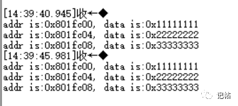
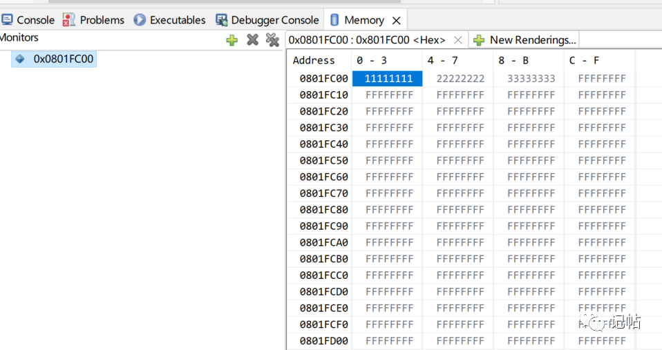
By checking the address in STM32CUBEIDE, you can also see that the value is written correctly.
Video
Continuously updating articles and learning materials, you can add the author’s WeChat for communication and study.
—QQGroup: 615061293—