According to the Cadence user guide, the Multi-bit flip-flop (MBFF) flow provides power optimization benefits with minimal impact on timing. This flow is utilized as part of the pre-CTS optimization stage.
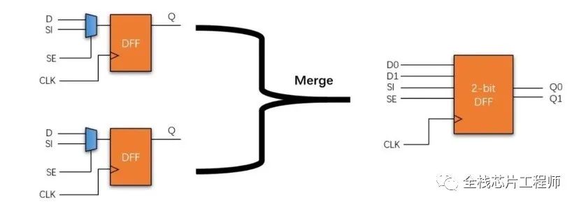
The term multi-bit cell can be understood as merging multiple identical cells into a single cell. As shown in the figure below, the clock inverter of a 2-bit multi-bit cell is shared, which saves the area and power of two clock inverters. Additionally, with a reduced number of flip-flops, the clock interconnect lines are also decreased, which reduces clock net length, capacitance, and clock inverter, further benefiting the overall power reduction.

It is crucial to note that the purpose of merging MBFF with SBFF is to reduce power consumption while ensuring timing is met. If timing requirements are not satisfied, MBFF should be split into SBFF, as SBFF is more convenient for resizing and moving operations.
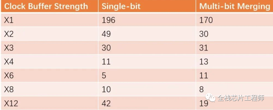
A significant portion of chip power consumption is attributed to the clock tree. By employing multi-bit cell technology, we can achieve the power improvements illustrated in the figure below:

Furthermore, scan DFFs typically have larger areas due to the inclusion of scan mux circuits. However, after merging single-bit registers, the Multi-bit flip-flop (MBFF) can significantly reduce area. For example, the logical relationship between single-bit and multi-bit DFFs is generally as follows:
During the layout design process at the transistor level, techniques such as optimizing transistor connections and sharing transistors are employed to save area. Therefore, the total layout area of multi-bit cells is smaller than that of an equivalent number of single-bit cells. Assuming the area of a 1-bit DFF is  , the area of a 2-bit DFF is generally smaller than
  , and the area of a 4-bit DFF is even smaller than
  .
.
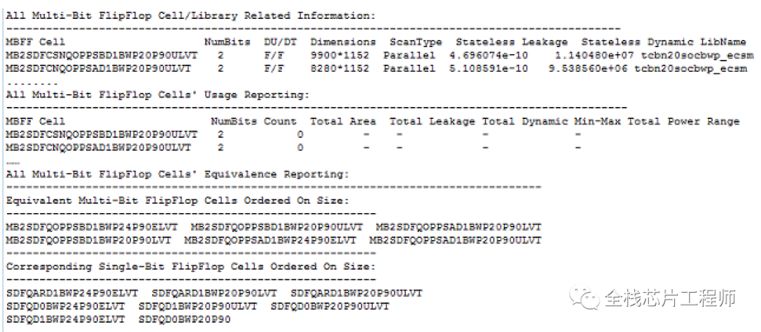
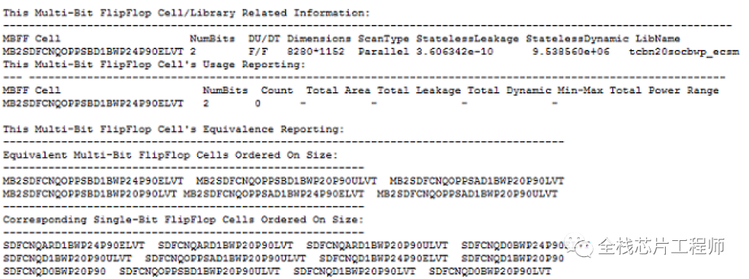
In Cadence INNOVUS, the following commands can be used to view MBFF information:
-
reportMultiBitFFs -all
-
reportMultiBitFFs -statistics

-
reportMultiBitFFs -cell MB2SDFCNQOPPSBD1BWP24P90ELVT
The benefits of the MBFF structure in terms of power consumption are primarily reflected in the following aspects: overall, it reduces clock net length, capacitance, and clock inverter.
1) Reduction of clock pin capacitance, thereby lowering clock switching power
As shown in the figure below, although the clock pin capacitance of a 2-bit MBFF does not significantly differ from that of a 1-bit flip-flop, when a large number of multi-bit DFFs replace single-bit DFFs in the design, the overall pin capacitance on the chip’s clock tree decreases significantly. The smaller the capacitance, the lower the switching power, resulting in reduced dynamic power consumption.

2) Reduction in the number of clock tree buffers, lowering switching and leakage power
Since the clock pin capacitance of each DFF in a multi-bit DFF is somewhat reduced compared to single-bit DFFs, a single buffer can drive more MDFFs in a multi-bit design. The primary reason is the reduced number of DFFs, which significantly decreases the number and area of buffers on the clock tree, further lowering power consumption on the clock tree.
3) Reduction in clock tree routing resources, leading to lower dynamic power due to parasitic RC
When MBFFs are extensively used, the number of standard cells in the chip decreases significantly compared to single-bit designs. Moreover, in many cases, the placement of DFFs may be more concentrated, saving substantial routing resources for the clock tree and consequently reducing the parasitic RC of the entire clock network. The figure below illustrates the routing differences between single-bit DFFs and multi-bit DFFs, showing that the routing of MBFFs on the right is noticeably less, thereby reducing the overall parasitic RC of the clock.

Despite the numerous advantages of multi-bit cells, optimal results are not always achieved in practical applications. The main reasons include the following: a) The conversion from single-bit to multi-bit has many conditional limitations, and often the actual ratio of multi-bit cells in the design is not high. b) Improper placement of multi-bit cells may lead to congestion and timing issues, potentially increasing the power of additional combinational logic, thus offsetting the power reduction benefits from the clock tree. For instance, if a 2-bit single-bit DFF is placed in different locations, merging it into a 2-bit multi-bit DFF may result in longer routing connections, increasing path delays. Tools may employ buffering and sizing optimizations to meet timing; if timing cannot be satisfied, it may be better to split the multi-bit cell into single-bit cells, as single-bit cells are more convenient for resizing and moving. c) Considerations regarding IR/EM may intentionally place multi-bit cells further apart, preventing the reduction of clock net length parasitic RC and thus failing to achieve the desired power reduction.